-

- News
- Books
Featured Books
- smt007 Magazine
Latest Issues
Current Issue
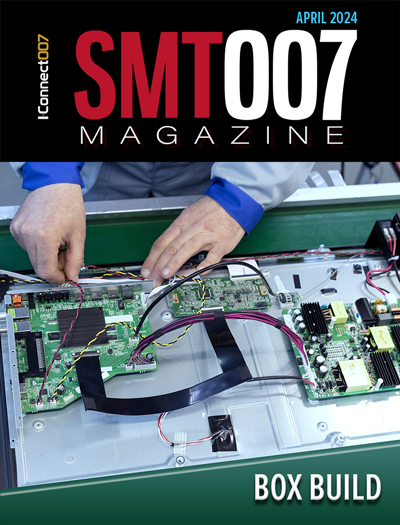
Box Build
One trend is to add box build and final assembly to your product offering. In this issue, we explore the opportunities and risks of adding system assembly to your service portfolio.

IPC APEX EXPO 2024 Pre-show
This month’s issue devotes its pages to a comprehensive preview of the IPC APEX EXPO 2024 event. Whether your role is technical or business, if you're new-to-the-industry or seasoned veteran, you'll find value throughout this program.

Boost Your Sales
Every part of your business can be evaluated as a process, including your sales funnel. Optimizing your selling process requires a coordinated effort between marketing and sales. In this issue, industry experts in marketing and sales offer their best advice on how to boost your sales efforts.
- Articles
- Columns
Search Console
- Links
- Events
||| MENU - smt007 Magazine
Saki Opens New Factory in Chiba, Japan
January 6, 2017 | Saki Corp.Estimated reading time: Less than a minute
Saki Corp. recently opened a new factory in Chiba, Japan to expand production of its automated inspection and measurement systems. Saki’s 2D and 3D automated optical inspection (AOI)and solder paste inspection (SPI), and 3D automated X-ray inspection (AXI) systems are used in printed circuit board assembly (PCBA) as well as for X-ray inspection of insulated gate bipolar transistors and sensors in automotive applications, especially in advanced driver assistance systems (ADAS).
"The requirements for increased inspection in the assembly of smartphones, communication servers, and automotive electronics to increase quality and eliminate device failure has created even more demand for our inspection systems," explained Nori Koike, COO, Saki. "Our new Saki Corporation Chiba Factory expands our production capacity and improves quality, cost, delivery for our customers."
Saki Corporation has headquarters in Tokyo, Japan; R&D, design, and engineering centers in Europe and China; and offices, subsidiary companies, and distributors throughout the world. Saki Corporation Chiba Factory was opened last December 20, 2016.
Suggested Items
ViTrox Technologies Elevates Service & Support Across US & Canada with Jeremy Woodworth's Appointment
04/18/2024 | ViTrox TechnologiesViTrox, which aims to be the World’s Most Trusted Technology Company, is pleased to announce the expansion of its US-based support team with the appointment of Jeremy Woodworth as Technical Support Senior Engineer based in the United States, effective March 15, 2024.
Yamaha to Showcase Latest-generation Assembly Equipment and Software Tools at SMTconnect
04/16/2024 | Yamaha Robotics SMT SectionYamaha Robotics SMT Section will team with its distributor ANS Elektronik to showcase innovations for high-speed surface mount assembly at SMTconnect 2024.
Marantz Electronics EZPro Software Solution: Streamlining Production Preparation for Cost-Efficient Manufacturing
04/16/2024 | Mek (Marantz Electronics)Marantz Electronics is proud to announce the launch of EZPro Software, Automatic Optical Inspection (AOI) machine programming that harnesses the power of Artificial Intelligence (AI).
Mek's Next-Gen AOI Technology Takes Center Stage at IPC APEX EXPO 2024
03/19/2024 | MEKMek is excited to announce its presence at IPC APEX EXPO, North America's largest electronics manufacturing event, in Anaheim, California, from April 6-11, 2024. Attendees are invited to visit Mek at booth #1433 to explore the latest AOI technology offerings.
New Features Boost Speed, Accuracy, Ease of Use for YAMAHA AOI System
03/18/2024 | Yamaha Robotics SMT SectionYamaha Robotics has announced Performance-boosting upgrades for the YAMAHA YRi-V 3D AOI system. These upgrades include faster board handling, multi-component alignment checking, and enhanced LED coplanarity measurement, among others.


