


 SMT Prospects and Perspectives: AI Opportunities, Challenges, and Possibilities, Part 1
 Nolan’s Notes: Do More, Get More
 Global Sourcing Spotlight: Don’t Be Afraid of Global Sourcing
Effect of Solder Composition, PCB Surface Finish and Solder Joint Volume on Drop-Shock Reliability
January 20, 2017 | Jim Wilcox and Francis Mutuku, Universal Instruments Corp.; and Shuai Shao and Babak Arfaei, Binghamton UniversityEstimated reading time: 5 minutes
Abstract
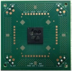
Drop shock reliability testing was performed on circuit boards assembled with several different lead-free solder alloys including SAC305 (Sn3.0Ag0.5Cu). The solder compositions tested range in Ag content from 0 to 3.0% by weight. Alloys with various secondary alloying elements were also included. All drop test boards were assembled such that the solder paste composition matched that of the BGA solder ball alloy to produce homogeneous solder joints of known compositions. An alternative test board design (not JEDEC standard) was used for this drop test evaluation. The test board contains a centrally located CABGA 256 package (17x17 mm body, 1 mm pitch). The board was designed with solder-mask defined pads to minimize the occurrence of pad cratering failure modes in the laminate material. The test package was soldered to the drop board using either BGA or LGA interconnections to explore the effects of solder joint volume. Drop shock events were characterized with acceleration monitoring on the drop table and strain gage measurements on the mounted test boards.
All samples were dropped until electrical failure. Solder joint microstructural analysis was performed on failing parts to establish the failure modes. The dominant failure mode was observed to be solder joint failure, either in the bulk solder or cracking along the interfacial intermetallic compound on the board pad. The effect of alloy silver content on drop reliability is noted. SAC305 solder joints were found to produce the best drop performance of all alloys tested for both BGA and LGA joint formats.
Introduction
Lead free solder joint reliability in drop shock loading has been a recurring issue in mobile and handheld consumer electronics. Changing solder composition may offer an opportunity to improve joint drop reliability. Low Ag alloys such as SAC105 have for instance been reported to have better drop performance than high Ag alloys such as SAC305. Some investigations suggested that this was because the failure mode changed from solder bulk failure (low Ag) to cracking of the interfacial intermetallic (high Ag). Others attributed it to a dominate failure mode of pad cratering for SAC105 on Cu-OSP, yet for SAC305 on Cu-OSP PCB surface finish failure was due to fracture of the Cu6Sn5 intermetallic compound (IMC).
Mattila4 explained that IMC cracking happens when the increased yield strength of the solder at high strain rate limited the strain accommodation provided by plastic deformation in the solder during the shock event. Thus, the brittle intermetallic layers failed due to increased stress concentration. Solder bulk failure on the other hand, occurred when solder strength was lower, usually the case for low silver alloys. Large plastic deformation in the solder reduces the overall stress in the connection and leads to a ductile bulk solder failure mode. Other researchers have reported that the strength response of SnAgCu solders may indeed vary by the drop acceleration level, increasing with the higher strain rates of large drop acceleration.
Tensile or peeling stress plays an important role in solder joint failure during the drop test. Typically, circuit boards are more flexible than the components attached to them. Considering that laboratory test assemblies are often dropped component side down with rigidly affixed board corners, the outermost solder joints will be under tension when the board flexes downward on initial impact. This tensile stress drives crack propagation of any crack initiated in the corner solder joints or in the underlying laminate. Joints at other locations may similarly fail but the outmost corner joints have the highest probability of producing the first failure.
Tensile test for bulk solder joints was performed at various strain rates and aging times by Luan, et al. Three failure modes of bulk solder were reported: brittle failure, ductile failure and mixed mode failure. Their reported data showed that higher strain rate led to statistically more brittle failure in the interfacial intermetallic compound. Longer aging time resulted in a thicker IMC layer and more brittle failure.
Solder alloys doped with various elements can lead to very different drop shock behavior. The effect of micro alloying elements on failure mechanism is not simple. For example, the effect of the addition of 0.1% Bi in high strain rate failures was dependent on the base alloy10. For low Ag alloys (Ag
Recently, new candidate board designs have been proposed as replacements for the JEDEC JESD22-B111 drop test board. Design changes were motivated primarily by concerns that the existing JESD22-B111 configuration does not provide the same stress distribution for all the components during drop, although some components are mounted symmetrically on board. Attributes of some of the new designs include a single component per board, four components per board mounted symmetrically or eight components mounted centro-symmetrically on a round test board. Another advantage of the new designs is that they usually have the board size close to that of hand-held portable devices, which can help provide a more realistic reliability assessment.
A common shortcoming of many developed interconnection reliability models is neglecting changes in failure modes. This makes the overall validity of these models questionable as drop tests producing different failure mechanisms are not simply comparable. This project is intended to study the failure behavior of several solder alloys in drop test. Each alloy is used to assemble LGA and BGA components on either a Cu-OSP surface finish board or an immersion silver surface finish board. The test board used is one redesigned from previous drop test efforts to influence the primary failure mode. Failure rates in drop shock are fitted to Weibull distributions for comparison. Characteristic failure modes for each solder alloy/board finish combination are identified.
Experiment Preparation
Test Board Assembly
A revised test board design is used for this study rather than the previously used JEDEC standard drop test board. In the multi-component JEDEC drop test board design, the stress distribution experienced during drop is not identical for all the components making analysis and interpretation of results difficult. The test board used is constructed of 6-layer 370HR laminate material with a body size of 77 x 77 mm. The boards were sourced with either Cu-OSP or immersion Ag surface finish.
The Chip Array BGA256 test component has a body size of 17 x 17 mm. The BGA footprint is full array with solder mask defined pads on a 1.0 mm pitch. The component surface finish is electrolytic NiAu. It is assembled to the test board in either the BGA or LGA (solder paste only) configuration.
To read this entire article, which appeared in the January 2017 issue of SMT Magazine, click here.
Share on:


Suggested Items
AIM to Highlight NC259FPA Ultrafine No Clean Solder Paste at SMTA Wisconsin Expo & Tech Forum
04/18/2024 | AIMAIM Solder, a leading global manufacturer of solder assembly materials for the electronics industry, is pleased to announce its participation in the upcoming SMTA Wisconsin Expo & Tech Forum taking place on May 7 at the Four Points by Sheraton | Milwaukee Airport, in Milwaukee, Wisconsin.
Hentec/RPS Publishes an Essential Guide to Selective Soldering Processing Tech Paper
04/17/2024 | Hentec Industries/RPS AutomationHentec Industries/RPS Automation, a leading manufacturer of selective soldering, lead tinning and solderability test equipment, announces that it has published a technical paper describing the critical process parameters that need to be optimized to ensure optimal results and guarantee the utmost in end-product quality.
Empowering Electronics Assembly: Introducing ALPHA Innolot MXE Alloy
04/16/2024 | MacDermid Alpha Electronics SolutionsIn the rapidly evolving electronics industry, where innovation drives progress, MacDermid Alpha Electronics Solutions is committed to setting a new standard. Today, we are pleased to introduce ALPHA Innolot MXE, a revolutionary alloy meticulously engineered to address the critical needs of enhanced reliability and performance in modern electronic assemblies.
New Book on Low-temperature Soldering Now Available
04/17/2024 | I-Connect007I-Connect007 is pleased to announce that The Printed Circuit Assembler’s Guide to… Low-temperature Soldering, Vol. 2, by subject matter experts at MacDermid Alpha Electronics Solutions, is now available for download.
Inkjet Solder Mask ‘Has Arrived’
04/10/2024 | Pete Starkey, I-Connect007I was delighted to be invited to attend an interactive webinar entitled “Solder Mask Coating Made Easy with Additive Manufacturing,” hosted by SUSS MicroTec Netherlands in Eindhoven. The webinar was introduced and moderated by André Bodegom, managing director at Adeon Technologies, and the speakers were Mariana Van Dam, senior product manager PCB imaging solutions at AGFA in Belgium; Ashley Steers, sales manager at Electra Polymers in the UK; and Dr. Luca Gautero, product manager at SUSS MicroTec Netherlands.