-

- News
- Books
Featured Books
- smt007 Magazine
Latest Issues
Current Issue
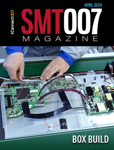
Box Build
One trend is to add box build and final assembly to your product offering. In this issue, we explore the opportunities and risks of adding system assembly to your service portfolio.

IPC APEX EXPO 2024 Pre-show
This month’s issue devotes its pages to a comprehensive preview of the IPC APEX EXPO 2024 event. Whether your role is technical or business, if you're new-to-the-industry or seasoned veteran, you'll find value throughout this program.

Boost Your Sales
Every part of your business can be evaluated as a process, including your sales funnel. Optimizing your selling process requires a coordinated effort between marketing and sales. In this issue, industry experts in marketing and sales offer their best advice on how to boost your sales efforts.
- Articles
- Columns
Search Console
- Links
- Events
||| MENU - smt007 Magazine
Goepel electronic Improves Inspection of Solder Pastes, DCB Substrates
June 7, 2018 | GOEPEL ElectronicEstimated reading time: 1 minute
Goepel electronic has upgraded the inline inspection system SPI Line · 3D. In addition to 3D solder paste inspection, the SPI Line · 3D now has new features for testing sinter pastes and direct copper bonded (DCB) substrates.
Due to the high precision of the system in conjunction with the new functions, process errors in sinter paste printing can now also be detected. Even the smallest defect structures such as voids and particles with heights below 20 µm can be detected with reproducible results. In addition, the system is now able to inspect DCB substrates. For example, air pockets (voids) on DCB structures can be reliably measured from a height of 10 µm. This makes the SPI Line · 3D the only SPI system currently available on the market that can be used for both traditional solder paste inspection with typical solder paste heights of 80 µm to 150 µm and for the newer applications of sinter paste and DCB testing with significantly lower structural heights.
The system software PILOT SPI provides the user with simple and intuitive test program creation. The operation is possible via touchscreen. Complete test programs can be created in less than 10 minutes.
The PILOT Connect software module connects the system with other inspection systems. This common interface for SPI, AOI and AXI centrally captures and manages all inspection data as well as the machine and operating data of the connected systems. It also allows bidirectional communication to higher level MES and traceability systems.
Furthermore, all inspection information can be merged on a central verification and repair station, combining data to create the safest and most dependable fault assessment environment available along with completely new possibilities for optimizing the production process.
Suggested Items
Hentec/RPS Publishes an Essential Guide to Selective Soldering Processing Tech Paper
04/17/2024 | Hentec Industries/RPS AutomationHentec Industries/RPS Automation, a leading manufacturer of selective soldering, lead tinning and solderability test equipment, announces that it has published a technical paper describing the critical process parameters that need to be optimized to ensure optimal results and guarantee the utmost in end-product quality.
Empowering Electronics Assembly: Introducing ALPHA Innolot MXE Alloy
04/16/2024 | MacDermid Alpha Electronics SolutionsIn the rapidly evolving electronics industry, where innovation drives progress, MacDermid Alpha Electronics Solutions is committed to setting a new standard. Today, we are pleased to introduce ALPHA Innolot MXE, a revolutionary alloy meticulously engineered to address the critical needs of enhanced reliability and performance in modern electronic assemblies.
New Book on Low-temperature Soldering Now Available
04/17/2024 | I-Connect007I-Connect007 is pleased to announce that The Printed Circuit Assembler’s Guide to… Low-temperature Soldering, Vol. 2, by subject matter experts at MacDermid Alpha Electronics Solutions, is now available for download.
Inkjet Solder Mask ‘Has Arrived’
04/10/2024 | Pete Starkey, I-Connect007I was delighted to be invited to attend an interactive webinar entitled “Solder Mask Coating Made Easy with Additive Manufacturing,” hosted by SUSS MicroTec Netherlands in Eindhoven. The webinar was introduced and moderated by André Bodegom, managing director at Adeon Technologies, and the speakers were Mariana Van Dam, senior product manager PCB imaging solutions at AGFA in Belgium; Ashley Steers, sales manager at Electra Polymers in the UK; and Dr. Luca Gautero, product manager at SUSS MicroTec Netherlands.
TE Connectivity Orders Hentec Industries/RPS Automation Pulsar Solderability Testing System
04/09/2024 | Hentec Industries/RPS AutomationHentec Industries/RPS Automation, a leading manufacturer of selective soldering, lead tinning and solderability test equipment, is pleased to announce that TE Connectivity has finalized the purchase of a Pulsar solderability testing system.


