


 SMT Prospects and Perspectives: AI Opportunities, Challenges, and Possibilities, Part 1
 Nolan’s Notes: Do More, Get More
 Global Sourcing Spotlight: Don’t Be Afraid of Global Sourcing
Evaluating the Impact of Powder Size and Stencils on Solder Paste Transfer Efficiency
July 31, 2018 | T. O’Neill, C. Tafoya, and G. Ramirez, AIM Metals and AlloysEstimated reading time: 9 minutes
Building upon an earlier study which focused on solder paste powder size, room-temperature aging and PCB pad and aperture designs, this study continues to investigate powder mesh size, but also examines stencil surface treatments and stencil foil tension. The goal of the study was to identify and rank the variables that provided the most improvement in repeatability, transfer efficiency and print definition for fine pitch printing. The results showed that nanocoating, powder type and tension rank highest to lowest in terms of their effect on print quality, and that high tension should be further studied to better understand where it makes the most significant impact.
Previous work revealed that:
a. reducing solder powder mesh size provides a modest improvement in print consistency and transfer efficiency for certain aperture designs
b. reducing solder powder mesh size may reduce solder paste useful life and increase process variables under certain conditions
c. pad and aperture design are the most significant variables in improving solder paste transfer efficiency when using high-quality, nanocoated stencils at standard mounting tensions
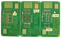
Figure 1: Jabil solder paste evaluation board.
This study adds to the database the effect of nanocoating and mounting tension on print quality, bringing a new arm to the experiment by printing unaged Type 4 (T4) and Type 5 (T5) solder pastes with similar stencils; however, one stencil is coated with a commercial polymer nanocoating and the other is uncoated and mounted at high tension. For reference, “standard” mounting tension is about 35N/cm, whereas “high” tension is 50N/cm or higher.
Theoretically, higher mounting tension should create Smore precise deposits because the foil will not deflect or reverberate as much during the separation phase of the printing process compared to a lower tension foil.
Experimental Method
Test Vehicle
The test vehicle (TV) selected for the print study was the Jabil Solder Paste Evaluation Board 2 that is commercially available from a leading dummy component and test kit supplier. The TV shown in Figure 1 provided an exceptionally thorough and detailed analysis in our earlier study and was used again in this study to provide continuity in data collection and analysis.
Features included:
• Print-to-fail (PTF) patterns with combined pad sizes ranging from 3 to 15mils with shapes including circular, square and rectangular pads, defined with both copper (NSMD) and solder mask (SMD)
• 0.4 and 0.5 mm BGA patterns.
• Markings on the PCB are etched in copper rather than silkscreened with ink to eliminate the standoff effect of PCB nomenclature
Table 1: Pad sizes, area ratios and theoretical aperture volumes for 4mil (100μm) foil.
The smallest feature size printed in this study was 6 mil (150 μm) which produces an area ratio of 0.38 using a 4 mil (100 μm) stencil. The smallest feature size reported is 8 mil (200 μm), as the variation increases dramatically below this threshold, due in part to the low ARs and in part to measurement error. The TV used in this arm of testing was from the same production lot that was used in the previous study. The data was collected using a new panel for each print. No PCBs were cleaned and reprinted. The pad and aperture sizes, area ratios and theoretical volumes are shown in Table 1.
Stencils
The stencils employed current state-of-the-art technology which would typically be used for the fine feature applications that demand finer powder solder pastes. They were cut from pre-mounted name-brand stainless steel on a modern, diode laser by a high-quality, US-based stencil supplier. One stencil foil was pre-mounted at high tension; the other at standard. The stencil supplier then applied a proprietary polymer nanocoating to the standard tension stencil. The SPI results from each stencil were compared to those in the existing database from the previous study. All apertures were sized one to one (1:1) with the test pads, with no reductions on any apertures.
Laboratory Equipment & Print Parameters
Figure 2: AIM applications laboratory manager reviews test setup.
The test equipment included a DEK Horizon screen printer, Parmi Sigma X SPI machine and ASH video microscope in the AIM Applications Laboratory located in Juarez, Mexico. The test area is climate controlled and can be manipulated to simulate production environments around the globe. Test conditions were optimized at 25.4°C (77.4°F) at 59% RH for these tests and recorded twice daily.
The facility is staffed with full-time SMTA-certified process engineers with over 50 years of combined experience in SMT assembly processes. Figure 2 shows the laboratory manager preparing the DEK Horizon printer and Parmi Sigma X SPI machine for the test run. The print parameters were as follows:
• Squeegee: 14” (355 mm) 60° angle DEK OEM
• Squeegee speed: 40 mm/sec (~1.6 in/sec)
• Squeegee pressure: 10 kg (~1.5 lb./in on 14” blades)
• Separation speed: 1 mm/sec (~0.040 in/sec)
• Separation distance: 3 mm (~120 mils)
• Under wipe sequence: Wet-Vacuum-Dry (WVD), using DEK EcoRoll wiper paper and AIM DJAW-10 solvent. Stencils were automatically underwiped before the first print of each set of five.
A dedicated flat tooling support block was used to provide solid support for the PCB, and new squeegee blades were used for the tests.
Automatic Solder Paste Inspection
SPI inspection parameters were modified to improve the accuracy of the measurements. Typically, a 30-40 μm measurement threshold is used in production environments to eliminate noise from PCBs’ topographical features like silkscreen markings, mask over trace, etc. Because the design of this TV limits topographical feature noise, it enabled a 15 μm measurement threshold, to improve measurement fidelity and aid in detecting subtle variations in print behavior.
Page 1 of 3
Share on:


Suggested Items
AIM to Highlight NC259FPA Ultrafine No Clean Solder Paste at SMTA Wisconsin Expo & Tech Forum
04/18/2024 | AIMAIM Solder, a leading global manufacturer of solder assembly materials for the electronics industry, is pleased to announce its participation in the upcoming SMTA Wisconsin Expo & Tech Forum taking place on May 7 at the Four Points by Sheraton | Milwaukee Airport, in Milwaukee, Wisconsin.
Hentec/RPS Publishes an Essential Guide to Selective Soldering Processing Tech Paper
04/17/2024 | Hentec Industries/RPS AutomationHentec Industries/RPS Automation, a leading manufacturer of selective soldering, lead tinning and solderability test equipment, announces that it has published a technical paper describing the critical process parameters that need to be optimized to ensure optimal results and guarantee the utmost in end-product quality.
Empowering Electronics Assembly: Introducing ALPHA Innolot MXE Alloy
04/16/2024 | MacDermid Alpha Electronics SolutionsIn the rapidly evolving electronics industry, where innovation drives progress, MacDermid Alpha Electronics Solutions is committed to setting a new standard. Today, we are pleased to introduce ALPHA Innolot MXE, a revolutionary alloy meticulously engineered to address the critical needs of enhanced reliability and performance in modern electronic assemblies.
New Book on Low-temperature Soldering Now Available
04/17/2024 | I-Connect007I-Connect007 is pleased to announce that The Printed Circuit Assembler’s Guide to… Low-temperature Soldering, Vol. 2, by subject matter experts at MacDermid Alpha Electronics Solutions, is now available for download.
Inkjet Solder Mask ‘Has Arrived’
04/10/2024 | Pete Starkey, I-Connect007I was delighted to be invited to attend an interactive webinar entitled “Solder Mask Coating Made Easy with Additive Manufacturing,” hosted by SUSS MicroTec Netherlands in Eindhoven. The webinar was introduced and moderated by André Bodegom, managing director at Adeon Technologies, and the speakers were Mariana Van Dam, senior product manager PCB imaging solutions at AGFA in Belgium; Ashley Steers, sales manager at Electra Polymers in the UK; and Dr. Luca Gautero, product manager at SUSS MicroTec Netherlands.