-

- News
- Books
Featured Books
- smt007 Magazine
Latest Issues
Current Issue
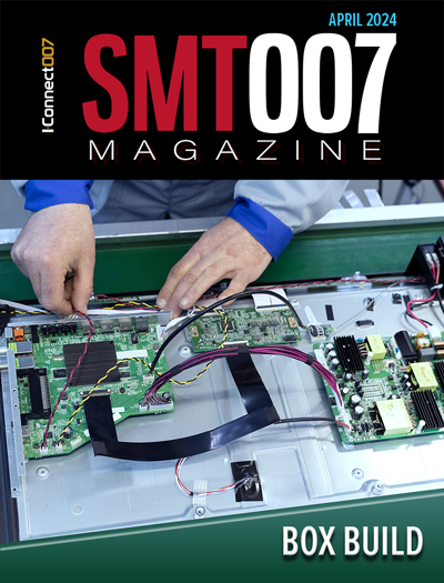
Box Build
One trend is to add box build and final assembly to your product offering. In this issue, we explore the opportunities and risks of adding system assembly to your service portfolio.

IPC APEX EXPO 2024 Pre-show
This month’s issue devotes its pages to a comprehensive preview of the IPC APEX EXPO 2024 event. Whether your role is technical or business, if you're new-to-the-industry or seasoned veteran, you'll find value throughout this program.

Boost Your Sales
Every part of your business can be evaluated as a process, including your sales funnel. Optimizing your selling process requires a coordinated effort between marketing and sales. In this issue, industry experts in marketing and sales offer their best advice on how to boost your sales efforts.
- Articles
- Columns
Search Console
- Links
- Events
||| MENU - smt007 Magazine
Practical Verification of Void Reduction Method for BTC Using Exposed Via-in-pad
December 16, 2019 | Alfredo Garcia, et al, Sanmina and NokiaEstimated reading time: 1 minute
Abstract
Void reduction strategies used with different levels of success throughout the industry include managing reflow profile parameters, solder paste deposit volume and solder paste type, stencil aperture cut to different geometries, thermal pad geometries with and without solder mask webs, vacuum-assisted reflow, sweep stimulation of PCB substrate, use of solder preforms, tinning of the components pads before placement and reflow, I/O aperture design to overprint at the toe of the pad, and exposed via-in-pad [1–8]. The translation of these methods and their combinations for void control on the thermal pad of bottom-terminated components (BTCs) has been met with different levels of success in volume production.
The method explored in this article regards the use of exposed via-in-pad. A dedicated test vehicle was designed for two types of QFN components. The main variables accounted for were the component size, number of exposed vias in the thermal pad, via pitch, via size, and solder paste coverage. The responses sought in this experiment include a thermal pad void level and solder wicking down the via barrel with resulting solder protrusion on the opposite side of the PCB.
The results indicated that solder will wick down the exposed via-in-pad regardless of the via diameter and solder paste coverage. Despite this finding, there were no defects recorded like component tilting, skewing, opens, or solder bridging. Specific configurations attained voiding levels in the thermal pad below 25%; however, other configurations did show a void level for the thermal pad up to 50%. A discussion will be presented regarding the effect of the board thickness and the geometry of the via array on the thermal pad solder coverage and voiding level.
To read this entire article, which appeared in the November 2019 issue of SMT007 Magazine, click here.
Suggested Items
AIM Solder’s Dillon Zhu to Present on Ultraminiature Soldering at SMTA China East
04/22/2024 | AIMAIM Solder, a leading global manufacturer of solder assembly materials for the electronics industry, is pleased to announce that Dillon Zhu will present on the topic: Ultraminiature Soldering: Techniques, Technologies, and Standards at SMTA China East. This event is being held at the Shanghai World Expo Exhibition & Convention Center from April 24-25.
AIM to Highlight NC259FPA Ultrafine No Clean Solder Paste at SMTA Wisconsin Expo & Tech Forum
04/18/2024 | AIMAIM Solder, a leading global manufacturer of solder assembly materials for the electronics industry, is pleased to announce its participation in the upcoming SMTA Wisconsin Expo & Tech Forum taking place on May 7 at the Four Points by Sheraton | Milwaukee Airport, in Milwaukee, Wisconsin.
Hentec/RPS Publishes an Essential Guide to Selective Soldering Processing Tech Paper
04/17/2024 | Hentec Industries/RPS AutomationHentec Industries/RPS Automation, a leading manufacturer of selective soldering, lead tinning and solderability test equipment, announces that it has published a technical paper describing the critical process parameters that need to be optimized to ensure optimal results and guarantee the utmost in end-product quality.
Empowering Electronics Assembly: Introducing ALPHA Innolot MXE Alloy
04/16/2024 | MacDermid Alpha Electronics SolutionsIn the rapidly evolving electronics industry, where innovation drives progress, MacDermid Alpha Electronics Solutions is committed to setting a new standard. Today, we are pleased to introduce ALPHA Innolot MXE, a revolutionary alloy meticulously engineered to address the critical needs of enhanced reliability and performance in modern electronic assemblies.
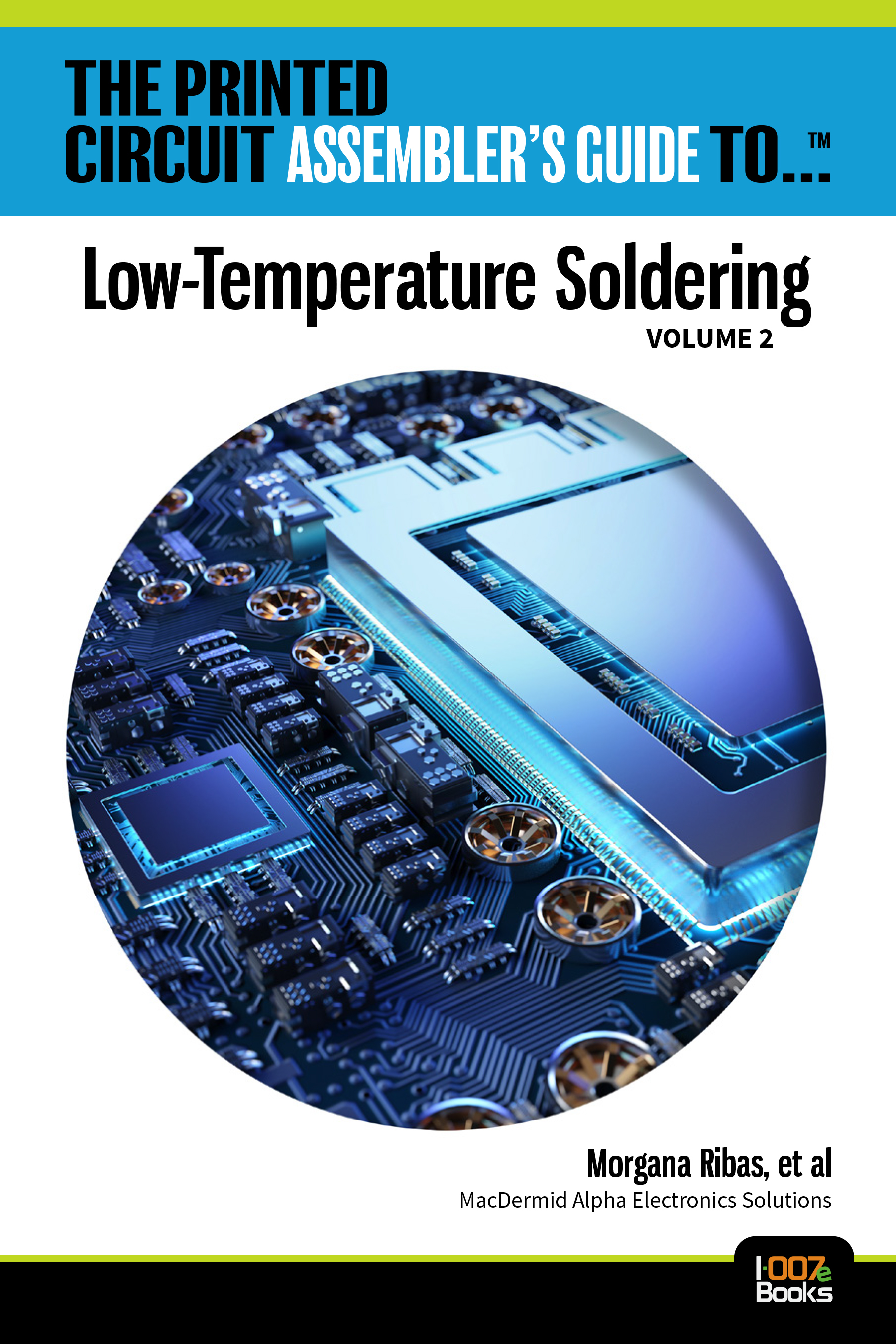
New Book on Low-temperature Soldering Now Available
04/17/2024 | I-Connect007I-Connect007 is pleased to announce that The Printed Circuit Assembler’s Guide to… Low-temperature Soldering, Vol. 2, by subject matter experts at MacDermid Alpha Electronics Solutions, is now available for download.


