


 SMT Prospects and Perspectives: AI Opportunities, Challenges, and Possibilities, Part 1
 Nolan’s Notes: Do More, Get More
 Global Sourcing Spotlight: Don’t Be Afraid of Global Sourcing
Forming Standards for Ultra HDI
October 25, 2022 | Andy Shaughnessy, Design007 MagazineEstimated reading time: 3 minutes

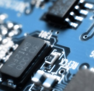
To get the latest news about ultra high-density interconnections (UHDI), we checked in with Jan Pedersen, NCAB Group’s director of technology. Jan is co-chair of IPC D-33AP, and a great source of overall DFM expertise as well. We asked him to give us a snapshot of UHDI in the industry, where we’re headed, and what this means to PCB designers.
Q: How do you define ultra HDI? What is the cutoff in mils or microns?
A: UHDI is defined in the IPC UHDI task group as a PCB design with lines and spaces below 50 microns, dielectric thickness below 50 microns, and microvias below 75 microns. These are attributes beyond the existing IPC-2226 Producibility level C.
Q: Tell us about your work on IPC’s UHDI committee. What are you working on right now? Are the standards keeping up with UHDI technology?
A: The UHDI task group has now developed a basic description and parameters. We are ready to hand over our work to the next group at IPC to start building the standards structure, starting with design, followed by performance and acceptance standards.
The standards will keep up with UHDI technology, but this will need our full attention for the standard to reflect current production capabilities globally.
Q: Much of the ultra HDI we see involves semi-additive technology. Can you clear up the differences between mSAP and A-SAP, and what it means to designers and design engineers?
A: SAP stands for semi-additive processes, and there are a few versions out there such as mSAP and A-SAP. We call them semi-additive because they all start with a thin layer of copper before creating the circuitry. This can be either from a copper-clad material, similar to what we use in traditional PCB manufacturing but with thinner copper, or a non-clad material where the PCB factory plates the seed layer. The difference between mSAP and A-SAP is the thickness of the seed layer where mSAP starts with a copper layer, typically 3–4 microns, while A-SAP starts from an unclad material activating the surface, adding a very thin chemical copper layer of less than 1 micron. Then both processes use photolithographic methods to plate up copper traces to around 20-micron thickness before flash etching the seed layer. Basically, the thickness of the seed layer, as we see with A-SAP, is the main factor for the process to create thinner traces.
Q: How is designing in the ultra HDI arena different from designing a typical PCB? What are some of the hurdles?
A: Designing ultra HDI is a challenge today because of a lack of standards, both for PCB production and material availability. The big hurdle today is fabrication availability. There are processes and some materials available, but very few PCB factories can offer anything below 40-micron trace and space. Some factories claim to offer UHDI, but that is very often only down to 35- to 40-micron traces, while the components you want to use requires traces and spaces below 30 microns.
Q: Are there any resources—books, websites, instructors, etc.—for UHDI design techniques?
A: For designers who want to learn more about UHDI, there are a limited number of resources. I would start with Tara Dunn’s Altium blogs and her I-Connect007 columns, which often cover semi-additive and UHDI. Anyone considering moving into ultra HDI should follow the NCAB blogs, available on our website and on LinkedIn. Read everything that you can.
Q: What advice would you give designers who are considering moving into UHDI?
A: The best advice I can offer is to find a supplier and be sure that you design within their capabilities. NCAB has a plan to be providing high-mix, low-volume UHDI starting as early as 2023. Today all factories that offer less than 35-micron traces have extremely long lead times. Not to sound commercial, but NCAB Group has a clear plan to change that. We are not there yet but will be very soon.
I am leading the NCAB Technical Council, and one of the focus teams is working actively with ultra HDI. As soon as we have a factory that can offer shorter lead times on UHDI, we will develop design guidelines and webinars, and provide workable parameters for designers. We need safe parameters to secure manufacturing yields and product quality from the start. It is paramount for NCAB Group to be transparent about what we can offer and how ready we are with new technologies.
This interview originally appeared in the October 2022 issue of Design007 Magazine.
Share on:


Suggested Items
Insulectro’s 'Storekeepers' Extend Their Welcome to Technology Village at IPC APEX EXPO
04/03/2024 | InsulectroInsulectro, the largest distributor of materials for use in the manufacture of PCBs and printed electronics, welcomes attendees to its TECHNOLOGY VILLAGE during this year’s IPC APEX EXPO at the Anaheim Convention Center, April 9-11, 2024.
ENNOVI Introduces a New Flexible Circuit Production Process for Low Voltage Connectivity in EV Battery Cell Contacting Systems
04/03/2024 | PRNewswireENNOVI, a mobility electrification solutions partner, introduces a more advanced and sustainable way of producing flexible circuits for low voltage signals in electric vehicle (EV) battery cell contacting systems.
Heavy Copper PCBs: Bridging the Gap Between Design and Fabrication, Part 1
04/01/2024 | Yash Sutariya, Saturn Electronics ServicesThey call me Sparky. This is due to my talent for getting shocked by a variety of voltages and because I cannot seem to keep my hands out of power control cabinets. While I do not have the time to throw the knife switch to the off position, that doesn’t stop me from sticking screwdrivers into the fuse boxes. In all honesty, I’m lucky to be alive. Fortunately, I also have a talent for building high-voltage heavy copper circuit boards. Since this is where I spend most of my time, I can guide you through some potential design for manufacturability (DFM) hazards you may encounter with heavy copper design.
Trouble in Your Tank: Supporting IC Substrates and Advanced Packaging, Part 5
03/19/2024 | Michael Carano -- Column: Trouble in Your TankDirect metallization systems based on conductive graphite or carbon dispersion are quickly gaining acceptance worldwide. Indeed, the environmental and productivity gains one can achieve with these processes are outstanding. In today’s highly competitive and litigious environment, direct metallization reduces costs associated with compliance, waste treatment, and legal issues related to chemical exposure. What makes these processes leaders in the direct metallization space?
AT&S Shines with Purest Copper on World Recycling Day
03/18/2024 | AT&SThe Styrian microelectronics specialist AT&S is taking World Recycling Day as an opportunity to review the progress that has been made in recent months at its sites around the world in terms of the efficient use of resources: