


 SMT Prospects and Perspectives: AI Opportunities, Challenges, and Possibilities, Part 1
 Nolan’s Notes: Do More, Get More
 Global Sourcing Spotlight: Don’t Be Afraid of Global Sourcing
Paper Substrates for RFID Tags
December 31, 1969 |Estimated reading time: 6 minutes
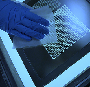
The first step to ultra-low-cost paper substrates for RFID tags is to demonstrate conductors on paper substrates from a processing standpoint, and characterize the electrical performance of paper substrates (up to 2 GHz) from a design standpoint. Conductors are achieved using conventional copper etching on laminated metal foils on paper substrates. There are several issues in optimizing the process such as copper bonding onto paper surfaces, adhesion, compatibility with copper-etch solutions, lithography, and moisture sealing. Despite obvious challenges, X/Y interconnects were successfully demonstrated on 12" × 12" paper substrates, which can be scaled to large-volume manufacturing. A ring resonator* was designed and fabricated to extract dielectric constants and losses. Copper metallization on paper substrates and the dielectric characterization of paper up to 2 GHz were reported. Antennas, copper conductors, resistors, capacitors, and inductors have been realized on paper substrates using conventional printed wiring board (PWB) process chemistries.
Paper is considered one of the best organic substrates for RFID tags. It is environmentally friendly and can undergo large reel-to-reel processing. It also is compatible with circuit printing using direct-write methods. This is one of its biggest advantages, because active tags require mounting or embedding of additional modules such as sensors and batteries. A fast ink jet printing process can be used efficiently to print these modules onto or into the paper substrate. Paper’s dielectric constant εr (~3) is close to that of air; therefore, electromagnetic power can penetrate it, even if the RFID is embedded.
The trend in RFID is toward achieving more functionality at a lower cost. More complicated RFIDs must be built with progressively lower-cost materials and processes that can be integrated with other surface or embedded modules. This article shows the path toward achieving conductive interconnects for the realization of complex circuitry on low-cost materials. Integrating RFIDs with paper-based pallets and containers would be a critical requirement for item tracking and inventory control in hospitals, supply chains, and aerospace. Thinner profiles also can be achieved with paper, enabling a new generation of wearable sensors.
Among the need to select the right paper are surface planarity, water-repelling properties, lamination for 3D module development, via-forming ability, adhesion, and co-processability with low-cost manufacturing. For trial runs, the selection was made using commercially available papers. Processes were developed for layer-to-layer lamination with inter-layer adhesion, copper-foil lamination, and etching.
 Figure 1. Ring resonator configuration.*
Conventional lamination and copper-etching chemistries have been adopted for high-volume, low-cost manufacturing. This is more operator-intensive, but can be adopted in a PCB fab house, and is more attractive for large-volume manufacturing. This method also has been optimized with five layers of laminated paper substrates with top and bottom layers of laminated 18-µm copper, followed by copper etching. A ring resonator with calibration lines was fabricated using conventional copper etching for dielectric characterization of paper substrates. The lamination process was optimized by varying temperature, pressure, residence time, and heating and cooling rates. The copper foil was bonded without any visible delamination or voids. The photolithography process was conducted using a dry-film photoresist, followed by UV exposure, and etching copper using a slow-etching chemistry. The laminated board was dried in an oven at 100oC for 30 minutes. Fabricated structures had good adherence to the paper substrate.
Measuring Dielectric Constant
This is a critical step to qualify paper material for a range of frequency-domain applications. Precise methods for high-frequency dielectric characterization include ring resonators, parallel-plate resonators, and cavity resonators. Such properties were not available for paper for the desired application frequency range (above 900 MHz). To measure the dielectric constant (εr) and loss tangent (tan δ) of paper up to 2 GHz, a resonator structure (Figure 1) was used with through-reflect-line (TRL) calibration to de-embed the effect of the feeding lines. However, tanδ extraction using the ring-resonator approach requires reliable theoretical equations to estimate conductor losses. Characterization covers the UHF RFID frequency band, which is used in applications for port security, inventory tracking, airport security and baggage control, automotive, and pharmaceutical/healthcare industries.
 Figure 2. S21 vs. frequency.
The ring resonator produces S21 results with periodic frequency resonances. In this method, εr can be extracted from the location of the resonances of a given radius ring resonator, while tanδ is extracted from the quality factor (Q) of the resonance peaks, along with theoretical calculations of conductor losses. Measurements of S21 were done over the frequency range 0.4 to 1.9 GHz using a Vector Network Analyzer (VNA).** Typical SMA coaxial connectors were used to feed the ring-resonator structure. TRL calibration was performed to de-embed the input and output microstrip feeding-line effects and eliminate impedance mismatches.
Figure 1 shows a layout of the ring resonator, along with dimensions for the microstrip feeding lines, the gap between the microstrip lines and the ring resonator, and width of signal lines. The mean radius rm S21 magnitude vs. frequency data were inserted into a Mathcad program, and the dielectric constant and loss tangent were extracted. A plot of S21 vs. frequency is shown in Figure 2.
Dielectric Constant
To extract the dielectric constant, the desired resonant peaks were first obtained according to:

where ƒo corresponds to the nth resonance frequency of the ring with a mean radius of rm and effective dielectric constant εeff, with c being the speed of light in vacuum. The extracted εr value at 0.71 GHz and 1.44 GHz (Figure 2) was obtained using equation 1, and is shown in Table 1.
The extraction of loss tangent was performed calculating the theoretical values of conductor and radiation losses. This isolates dielectric loss αd, since the ring-resonator method gives the total loss at the frequency locations of the resonant peaks. The loss tangent is a function of αd (in Nepers/m) according to:

where λo is free-space wavelength, εr and εeff are the same as described above. Tanδ results are shown in Table 1, minus calculated conductor and radiation losses.
3D Paper-on-Paper
To achieve 3-D paper-on-paper structures (similar to LTCC approach) with embedded passives, MEMS, RFIDs, sensors, thin-film batteries, and discretes and ICs, several bottlenecks need to be overcome, as none of these processes have been optimized or addressed. Possible bottlenecks include the production of thick substrates using a conventional lamination process; the formation of conductor lines, via formation for layer-to-layer connectivity; realization of passives such as resistors, inductors, and capacitors; formation of complex antenna structures; cavity formation for embedding chips; and thermo-mechanical integrity. For example, parallel-plate capacitors were fabricated on a paper substrate using copper-foil lamination and etching. Resistors and inductors were also fabricated on the laminated paper substrates using copper lamination and etching, then polymer thick films were screen printed. Through lamination and selective etching, resistors, capacitors, and inductors have also been realized on one layer using copper and pre-deposited resistor film on copper foil. They were laminated to form a multilayer structure with cut-out cavities for embedding ICs.

ConclusionIn a cost-driven market, ultimate success depends on selecting the lowest-cost materials and manufacturing processes. Embedded components, actives, sensors, and RFIDs for wireless sensing can be adopted in applications serving supermarkets to bio-hazards, security, medical, and defense applications. This article looks at applying paper-based substrates for functional circuitry. A 3D paper-on-paper package similar to LTCC green sheets is under construction. The outcome would be a flexible 3D package with embedded actives and passives and a thin-film battery in a paper substrate. This is expected to be the lowest-cost solution for wireless sensing with RFID tags for large-volume applications.*Microstrip ring resonator.**Agilent 8530A Vector Network Analyzer.
AcknowledgmentsCabot Corp. provided conductive inks; Dimatix provided technical support.
REFERENCESFor a complete list, contact the authors.
Swapan K. Bhattacharya, Amin Rida, Manos M. Tentzeris, Rushi Vyas, and Li Yang work at the PIREA RFID/Sensor Lab, School of Electrical and Computer Engineering, Georgia Institute of Technology. Contact Swapan K. Bhattacharya at swapan@ee.gatech.edu.
Share on:


