


 SMT Prospects and Perspectives: AI Opportunities, Challenges, and Possibilities, Part 1
 Nolan’s Notes: Do More, Get More
 Global Sourcing Spotlight: Don’t Be Afraid of Global Sourcing
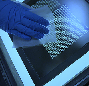
PRINTING MINIATURIZED COMPONENTS
December 31, 1969 |Estimated reading time: 11 minutes
By Clive Ashmore and Jeff Schake, DEK International
Moore’s Law governing chip density is just one of the curves defining the ongoing miniaturization of electronic products. Advances in component packaging, high-density board fabrication, and system-level integration contribute to overall progress. Shrinking I/O and connector pitches; consolidation of board-level interconnects using technologies such as via-in-pad; and a reduction in standard surface mount device (SMD) form factors from 0201 to the emergence of 01005s, are some examples of the ingenuity applied to all levels of assembly.
But manufacturers must be able to work with these technologies as part of an in-line, automated progression toward the end-of-line, to achieve efficient production at high rates of yield and throughput. Since the indicators for end-of-line yield are set at pre-placement, it is important to understand how accepted screen printing practices should change to accommodate the latest package styles and board-design techniques.
Recent work has analyzed the impact of 0.3-mm-pitch chip-scale packages (CSPs), as well as SMD resistors in the 01005 EIA form factor, on printing processes, including printer set-up, stencil design, and solder paste formulation. The 0.3-mm CSP represents a major evolution within the SMT arena. This device will require arrays of mass-imaged solder paste at pitches and volumes that previously would have warranted a “semiconductor” classification. Challenges include sub-7-sec. cycle times used in surface mount production; thin, often uneven FR-4 boards generally used in SMT; and standard working environments of a typical assembly operation. By comparison, semiconductor packaging processes have the benefits of slower cycle times, perfectly flat wafers, and clean-room environments.
Among surface mount passives, the industry-standard 0201 outline for resistors and capacitors continues to grow in popularity to meet more strict form-factor design constraints. The smaller size option - 01005 - is being designed into advanced assemblies. Uncertainty surrounding the impact on issues such as stencil aperture characteristics and solder paste transfer efficiency has fueled fears of the return of tombstoning, resulting in defective assemblies post-reflow.
 Figure 1. Aperture sizes calculated from established dimensions for 0201 production; standard and overprint aperture sizes; effects of low, medium, and high stencil grab; and variations in print offset.
Whatever the effect of any of these issues, and the performance of any solutions developed, SMT assemblers need to build complete boards in a unified, end-to-end sequence to maintain throughput and minimize cost per assembly. Before these packages can be adopted in mainstream SMT assembly, manufacturers need assurance that practicable production processes can be established.
Printer Performance
Screen printing technology has already shown an ability to keep pace with advances in electronics assembly. Cutting-edge screen printing platforms are being adopted throughout the semiconductor industry to perform package assembly processes at the finest interconnect pitches in use, including wafer bumping, solder ball attach, and precision wafer coating for die attach. Major semiconductor brands as well as the non-captive packaging sector have implemented production processes capable of high throughput to build the CSPs entering volume SMT production. Absolute accuracy of screen printing platforms at board-level resolutions is not in doubt. Instead, questions center on establishing optimal specifications for solder paste, stencil technology, design rules, and acceptable quality standards for PCBs.
Screen Printing 01005 Passives
Recent work investigated the effects of solder pad layout, stencil design, and solder paste characteristics and reflow conditions on assembly of components marketed in the 01005 package outline.1 Analysis focused on a spread of aperture sizes calculated from established dimensions for 0201 production; the use of standard and overprint aperture sizes; the effects of low, medium, and high stencil grab; and variations in print offset (Figure 1).
 Figure 2. Tombstoning for 01005 and 0201 components.
This work has successfully challenged the belief that 01005 devices would be particularly prone to tombstoning. In fact, results achieved by deliberately printing paste onto only one pad to set-up the most extreme imbalance of wetting forces during reflow showed an inherently lower tendency toward tombstoning compared to 0201 components (Figure 2). When normal stencils were used to deposit solder paste at each pad site and reflow 01005s successfully, measures including the use of nitrogen-rich reflow atmosphere and 90° component orientation were used to maximize the possibility of tombstoning. Both of these factors are proven to lead to higher instances of tombstone defects with 0201 passives. In 01005 experiments, no significant instances were recorded, indicating that 01005 components tested were inherently less vulnerable to mechanisms that produce tombstoning. A sample of 01005 resistors were also assembled at 0° orientation to determine orientation sensitivity. No influence on assembly yield was observed.
 Figure 3a. Stencil A.
Over-sized aperture designs were also tested, and demonstrated high and repeatable rates of solder paste transfer efficiency. However, experimentation with a wide range of aperture sizes and pad layouts showed that this approach is not necessary to achieve satisfactory yield. Moreover, delivering excess solder to the pads in this way produced bulging solder joints as well as instances of floating components.
 Figure 3b. Stencil B.
Grab, in relation to stencil design, is the amount of overlap provided between the termination of a passive component and printed solder paste. The larger the overlap, the greater the tendency for solder paste to grab the termination during reflow. In practice, the grab experienced at each termination of a given component depends on stencil aperture sizes and positions, as well as the distance separating two solder pads. After analysis, a high-grab stencil design, combined with the lowest pad-separation distance, could tolerate ±20-µm print and ±60-µm placement mis-registrations, while still achieving sufficient contact between component terminations and solder paste to ensure satisfactory results after reflow.
 Figure 3c. Stencil C.
Another issue is that, when using a standard laser-cut stainless steel stencil of 100-µm thickness, the height of the solder paste deposit is close to that of the 01005 resistor. As the component is inserted into the paste, it is possible for solder paste displaced by this action to contaminate the placement nozzle. The consequences of this include significant pick-yield loss, requiring frequent machine stops to clean the nozzle. Nozzle contamination was highest at high pad separation and low stencil grab. There is also scope for enhanced nozzle-tip designs to reduce the occurrence and offset the effects of solder paste contamination.
When reflowed in air, satisfactory results were achieved using standard Type 3 lead-free solder paste, combined with 100-µm laser-cut stencils, subject to optimization of stencil design in relation to pad layout. Instances of tombstoning are comparable to those experienced using 0201 components. However, using a nitrogen-rich reflow environment has been shown to reduce tomsbtoning significantly with 01005s.
In general, air is preferred for reflow, and the fact that 01005 passives have been assembled successfully in this type of environment is reassuring for those looking to introduce assembly processes using 01005s. On the other hand, some instances of incomplete solder coalescence were observed, indicating that more work is required to investigate the reflow behavior of very low volumes of solder paste.
Paste Particle Size
The progressive reduction of interconnect pitch is a dominant feature of typical CSP roadmaps. Beginning at about half the typical pitch for BGA packages aimed at the handheld market, CSP pitches are 0.4 mm, and moving to 0.3 mm.2 Evaluation of 0.3-mm-pitch CSP assembly has established recommendations on solder paste type, stencil technology and thickness, and aperture dimensions.3 This work has shown that it is possible to achieve high yields using the latest CSPs at cycle times as low as seven seconds. This rapid cycle time is necessary to allow 0.3-mm CSP assembly to be integrated into a modern, high-volume assembly line.
 Figure 4. Number of failed interconnects vs. stencil and area ratio (Type 3 solder paste)
Of stencil types evaluated, 50- and 75-µm laser-cut stencils, as well as a 67-µm electroformed stencils, were most successful. Figures 3a-c show the shapes and sizes of apertures tested. Investigation into optimal aperture dimensions included a range of circular aperture designs centered on the IPC-7525 area ratio specification. It is critical to prove that a satisfactory aperture ratio can be found to show that 0.3-mm-pitch CSPs can be assembled alongside conventional components within the same process.
In addition to investigating process performance using Type 3 solder pastes, this work also recorded results using a Type 4 paste containing smaller particle sizes. Among the observed results, the Type 3 solder paste produced satisfactory results subject to a number of caveats on stencil design. Predominantly, the rule that requires aperture ratio to be greater than 0.66 must be followed. With this in mind, a combination of 50-µm stencil thickness and 180-µm aperture diameter would deliver satisfactory results for 0.3-mm-pitch CSPs. However, this would promote defects with other package types on the same board by preventing the use of aperture sizes adequate enough to deposit sufficient paste volumes. Because the desire is to discover recommendations for a process supporting multiple package technologies, the use of Type 3 paste with 50-µm stencil thickness is unsatisfactory.
Increasing stencil thickness to 75 µm would improve process performance for other technologies, but would require aperture diameters greater than 200 µm to maintain the area ratio rule for 0.3-mm-pitch CSPs. These apertures are large enough to cause solder paste bridging.
Changing to Type 4 solder paste allows a wider process window, resulting in lower defect rates with a reduced area ratio. Figures 4 and 5 show the numbers of failed interconnects detected vs. stencil type and area ratio for Types 3 and 4 pastes. The results show that, when using Type 4 paste, it is possible to use a 75-µm-thick stencil with aperture diameters ranging from 170 to 190 µm, and low numbers of defects recorded for CSPs. The 75-µm stencil is better for overall performance, including mature package types.
 Figure 5. Number of failed interconnects vs. stencil and area ratio (Type 4 solder paste)
Observations on stencil manufacturing technology are also interesting for assemblers looking to implement a process for 0.3-mm-pitch CSPs. In general, migration to finer interconnect geometries is believed to demand adoption of enhanced stencil technologies such as electroforming. Close-up aperture images in Figure 3a-c show that electroforming does produce smoother and more uniform apertures. However, experimental results demonstrate that stencil technology has a lower influence when using Type 4 paste. Therefore, 0.3-mm-pitch CSPs can be incorporated into an existing process successfully, with few changes. Deposits can be printed using high-quality laser-cut stencils with a thickness appropriate to more mature package technologies at a lower-than-standard area ratio to avoid excessive paste volume. Using a Type 4 solder paste is advisable, and provides protection against insufficient-type defects at CSP pad sites.
Conclusion
At first consideration, advanced package technologies may appear to require a quantum leap in materials and process parameters to establish manufacturability. As a body of practical experience is gathered, more straightforward solutions emerge. In practice and production, satisfactory results have been achieved with the latest 01005 passives and 0.3-mm-pitch CSPs. A successful 01005 resistor assembly process has been demonstrated using a 100-µm-thick stencil with Type 3 lead-free alloy solder pastes across a variety of Cu/OSP pad sizes. A standard reflow process produces a similar number of tombstone defects as with 0201s; using a nitrogen-rich atmosphere reduces tombstoning with 01005s.
Type 3 pastes can be used in the 0.3-mm CSP assembly process, producing satisfactory yields, provided the IPC-7525 area ratio rule of greater than 0.66 is followed. For a wider process window, suitable for high-volume assembly of production boards using a variety of component technologies, Type 4 paste is recommended. Combined with a 75-µm stencil, a high-quality laser-cut or electroformed stencil, and aperture diameters ranging from 170 to 190 µm, these represent the best set of materials and conditions for 0.3-mm-pitch CSP pre-placement. Further investigation is required into the effects of squeegee characteristics and reflow atmosphere. Generally, as with all leading-edge processes, the primary recommendation when seeking to optimize for high-volume production is to secure the fullest possible understanding of materials and mechanisms involved.
REFERENCES
- Schake, Jeff, “Mass Reflow Assembly of 01005 Resistor Components,” APEX 2007.
- iNEMI Packaging Roadmap Overview, 2005.
- Ashmore, Clive, “Investigation into the Mass Imaging Aspects of 0.3-mm Wafer-level CSP Solder Paste Deposition,” APEX 2007.
Clive Ashmore, global applied process engineer, DEK, may be contacted at cashmore@dek.com. Jeff Schake, senior advanced technology specialist, DEK, may be contacted at jschake@dek.com.
Printed Electronics Hold Exciting Possibilities
Imagine product packaging with dynamic images that move and change colors, attracting the attention of consumers. Or imagine sensors printed on food packaging that indicate freshness levels, and warn when food is past its expiration date. Now picture the ability to print solid state lighting on easy-to-dispense rolls of paper or plastic. All of these are possible with printed electronics. By combining novel electrically functional inks (conductive, semiconductive, and dielectric) with graphic arts printing platforms (gravure, flexography, ink jet), both active and passive devices can be produced with extremely high throughput at very low cost.
Semiconductor devices and circuits with feature sizes approaching 10 µm or smaller potentially can be printed. There are many applications where low-cost and high-speed production trumps the need for fine circuitry. There also are many products that do not integrate electronics, but could benefit from their functionality.
The latest iNEMI Roadmap includes a chapter on printed and organic electronics. As this industry establishes itself, it is critical to develop a robust supply chain, and identify the gaps/needs of enabling technologies. The Roadmap identifies the following elements as most important for supply-chain development:
Materials - Charge-carrier mobility and relatively large operational voltage (compared to silicon) limit the breadth of applications that can be printed. Performance is sufficient for some applications (such as bi-stable displays used for e-books), but the ultimate impact of the technology would be improved with the advent of higher-mobility inks.
Equipment platforms and control architectures - Existing processing equipment must be improved to achieve finer printed circuit resolution. There also is a need for advanced in-line and off-line control systems for high-yield manufacturing.
System testing - Production volume of printed electronics is several orders of magnitude greater than typical consumer electronics manufacturing lines (i.e. hundreds of meters/minute, or thousands of sheets/hour), which raises questions regarding testing. New test standards and equipment must be developed to ensure quality control.
Design and application - Design tools are needed for printed electronics products. Some have suggested that existing software packages can be adapted, while others argue that new tools must be developed.
Daniel Gamota, director of Motorola’s Printed Electronics Group and chair of the Organic & Printed Electronics Chapter of the 2007 iNEMI Roadmap, may be contacted via e-mail: gamota@motorola.com. For information on the iNEMI Roadmap, visit http://www.inemi.org/cms/roadmapping/2007_iNEMI_Roadmap.html.
Share on:


