


 SMT Prospects and Perspectives: AI Opportunities, Challenges, and Possibilities, Part 1
 Nolan’s Notes: Do More, Get More
 Global Sourcing Spotlight: Don’t Be Afraid of Global Sourcing
Choosing a Stencil
December 31, 1969 |Estimated reading time: 10 minutes
Is a stencil a commodity or a precision tool? A commodity is something that can be purchased from many suppliers, with the expectation that the performance will be the same. A precision tool is designed to perform a specific task, which, In the case of stencil printing, is to provide defect-free printing. This article examines how to choose a precision stencil tool for printing.
By William E. Coleman, Ph.D. and Michael R. Burgess
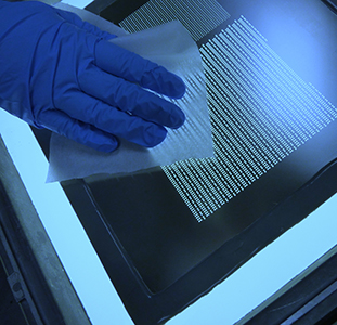
In light of recent demanding requirements of lead-free printing and ultra-fine-pitch printing of devices such as 0.4-mm microBGAs and 0201 chip components, a precision stencil tool is required. The function of a stencil is to deposit solder paste, conductive polymer, glue, or flux onto a substrate. Generally, the substrate is a PCB, but a silicon wafer is also used for printing solder paste onto wafer pads for wafer bumping. Ball-placement tools - although not specifically considered stencils - fall into the stencil domain. Instead of transferring paste through stencil apertures, solder balls are positioned over a wafer or BGA substrate through stencil apertures. For paste printing, the stencil printing process can be divided into three categories: the aperture-fill process, the paste-transfer process, and the positional location of the deposited paste. All three processes play a vital role in achieving the desired result - a precise volume of paste (a brick) deposited to the correct location on the substrate.
 Figure 1. Laser-cut, no surface treatment, side wall.
The first step in printing solder paste is to fill the stencil aperture with paste. This is achieved using a metal squeegee blade. Several factors can contribute to the aperture-fill process. The orientation of the aperture with respect to the squeegee blade has an effect on the fill process. An aperture oriented with its long axis in the same direction as the blade stroke does not fill as well as an aperture oriented with its short axis to the blade stroke. Squeegee speed also influences aperture fill. Squeegee speed must be reduced to fill the aperture with the long axis oriented parallel to the squeegee stroke. The squeegee-blade edge has an influence on how well the paste fills a stencil aperture. The rule of thumb is to print at the minimum squeegee pressure while still maintaining a clean wipe of the solder paste on the stencil surface. If squeegee pressure is too high, both the squeegee blade and the stencil may be damaged. Excessive squeegee pressure can also cause paste smearing under the stencil surface. If the pressure is too low, one of two events may occur. Paste left on the squeegee side of a small aperture will hold the paste, preventing its release to the PCB pad, resulting in insufficient solder. Paste left on the squeegee side over large apertures will be pulled down through the aperture, resulting in excess solder. Proper squeegee pressure is the minimum pressure that achieves a clean wipe of the paste. Minimum pressure is a function of blade type. A recent study demonstrated that the minimum squeegee pressure for one squeegee blade* was about 40% of that of the teflon/nickel-coated blade for lead-free solder paste. Tests have confirmed that lead-free solder pastes typically require about 25% more squeegee pressure than tin/lead pastes.
 Figure 2. Laser-cut, electro-polished side wall.
There are two primary considerations for solder paste release: the area ratio/aspect ratio for stencil design and the type of stencil. The first is a function of stencil design, while the second is a function of aperture-wall smoothness and side-wall geometry. The aspect ratio is the width of the aperture divided by stencil thickness. It is generally accepted that an aspect ratio of 1.5 or greater should achieve acceptable solder paste transfer. The aspect ratio is a useful guide when the aperture length (L) is much larger than aperture width (W), such as greater than 5× the width. BGAs, microBGAs, and 0201s have aperture dimensions where L and W are close to the same value. These apertures are either circles and squares, or oblongs and squares with radius corners. In all cases, the length is much less than 5× the width. It is more common to use the area ratio as a guide to paste-transfer efficiency. The area ratio is the area beneath the stencil aperture opening, divided by the area of the inside aperture wall. For a rectangular aperture, the area ratio = [(L×W)/2(L+W)T)], where L and W are the aperture length and width, respectively, and T is stencil thickness. For a square aperture, area ratio = S/4T, where S is the side of the square. For a circular aperture, area ratio = D/4T, where D is the diameter of the circle. The generally accepted rule is to achieve area ratios of >0.66 for paste transfer. This was true until the advent of electroformed stencils. It is common with this technology to print apertures with area ratios down to 0.50. One electroformed stencil** with relatively straight side walls and a smooth mirror-like finish promotes greater solder paste release, which is helpful as component sizes and pitches continue to decrease.
There are two primary stencil technologies used within the industry: electroformed and laser-cut. Chemical etching can also be used to create steps for step stencils; however, final stencil apertures are generally laser-cut. Three-dimensional (3-D) electroformed stencils are also available for use when unique steps are needed, providing release qualities required for fine-feature printing.
 Figure 3. Laser-cut, electro-polished, nickel-plated side wall.
Laser-cutting is a subtractive process. Traditional Gerber files are converted to CNC-type language files that the laser can interpret. The final aperture shape and smoothness is impacted by a laser-cutting machine, cut speed, laser power, beam spot size, and beam focus. Some laser-cutting machines are homemade systems, some vintage lasers, and some are fine-cut laser machines. Electro-polishing and nickel-plating are also used to further smooth surface walls and improve solder paste release. Figures 1-3 demonstrate how successive surface treatment can smooth out the surface wall to improve paste release. As a minimum, a stencil supplier should electro-polish the laser-cut stencils.
Electroformed stencils are made by using an additive process. A nickel bath containing nickel ions and a nickel-hardening additive is plated onto a mandrel to form the stencil. The process begins by applying photo-resist to the mandrel. Next, a photo tool is plotted and placed over the resist-coated mandrel. The resist is exposed and developed, creating small pillars of solder-resist similar to solder paste bricks. As with any photolithographic process, a clean-room environment with tight particle count and size control, as well as tight temperature and humidity control, is needed to produce a high-quality electroformed stencil. Nickel is electroplated out of the bath onto the mandrel one ion at a time around resist pillars until the desired thickness is achieved. The resulting stencil has smooth, straight-wall apertures (Figure 4) that are precisely located and capable of printing area ratios down to 0.50.
 Figure 4. An electroformed stencil side wall.
An understanding of stencil-design factors impacting solder paste release is imperative to print any solder paste successfully. The lead-free movement adds another variable that was not fully understood in the early transition stages. It has been demonstrated that paste-transfer efficiency is higher for tin/lead solder paste than lead-free. Therefore, stencil technology selection will become more critical in achieving the best solder paste release and maximum transfer efficiency. Using area ratio calculations will help designers and process engineers when selecting the proper technology. When the area ratio is greater than 0.66, most laser-cut stencils can be used successfully. However, if component and pad geometries require designs with area ratios between 0.50 and 0.66, electroformed stencils should be considered. Figure 5 shows stencil recommendations for a 5-mil-thick stencil. Curves are drawn for area ratios of 0.5, 0.66, and 0.9.
 Figure 5. Area ratio chart with stencil technology recommendation.
If a particular aperture size lies below the 0.5 curve, aperture redesign is recommended by either decreasing stencil thickness or increasing aperture size. If aperture design lies between 0.5 and 0.66, an electroformed stencil is recommended. Another useful tool is an area ratio calculator,*** which gives the area ratio as an output once aperture size and stencil thickness are inputted. An additional output of the area ratio calculator is recommended on stencil technology. An example is the design of a stencil for printing 01005 chips. For a circular or rounded square aperture of 7 mils., with a stencil thickness of 3 mils., the area ratio is 0.583; an electroformed stencil is recommended.
Aperture Positional Accuracy
The positional accuracy of an aperture in the stencil determines how accurately a solder brick is placed onto the PCB pad. Although this is important for tin/lead processes, it is even more critical for lead-free processes. Printing off-pad can contribute to failures such as solder balls, tombstones, opens, and shorts. Lead-free solder pastes do not wet and spread as well during reflow. If the solder brick does not cover all of the pad, the paste typically will not flow out and cover that portion of the pad.
Positional accuracy in a stencil is tied to the manufacturing process. In laser manufacturing, the X/Y movement of the cutting beam must be controlled. Another factor is any stretching of the pattern during stencil cutting or while mounting the stencil foil in a frame. This is especially true for thin stencils having many apertures (a high percent of open foil area). The manufacturing process is different for electroformed stencils. A photo tool is used to create the photo-resist pillars that form apertures as nickel plates up around the pillars. The photo tool must be processed and imaged in a tightly controlled temperature and humidity environment. Any distortion (stretch/shrink) during electroforming or mounting processes must be compensated for during the photo-tool creation. A recommended specification for both laser and electroformed stencils is distortion (stretch/shrink) of <0.1 mils. per inch of an aperture pattern in X and Y. Good process control during stencil manufacturing is necessary to meet this standard. It also is important for the stencil vendor to certify the positional accuracy of each stencil shipped with the appropriate high-end optical measuring equipment. It is possible to scale the stencil to match the board to achieve positional accuracy. The stencil vendor who measures the board performs this and creates a new stencil Gerber file to match the board. Typically, large boards (~18" × 24") using lead-free solder paste may need stencil scaling to match the board.
Choosing a Stencil
Do all electroformed stencils perform alike? What about laser stencils? How can true stencil performance be determined? The stencil end-user could conduct an in-house performance evaluation for a number of stencils, or have an independent test laboratory do so. One method would be to have various stencil vendors manufacture a stencil using the exact same Gerber file, and compare stencil-print performance of each stencil. A recent study by an independent test laboratory evaluated 12 stencils from 5 stencil vendors. Print performance was judged by solder paste transfer and volume repeatability, as well as aperture positional accuracy. Five electroformed stencils and seven laser-cut stencils were supplied. The electroformed stencils are labeled 1, 3, 5, 7, and 9. Laser-cut stencils were labeled 2, 4, 6, 8, 10, 11, and 12. Laser-cut stencil 2 was nickel-plated, while laser-cut stencil 11 was cut in an electroformed foil. Solder paste volume was measured for 16 different SMT components including 0.4- and 0.5-mm microBGAs, 0201s, and 0.4- and 0.5-mm-pitch quad flat packs (QFPs). Both tin/lead and lead-free solder paste was used. A ranking system was devised in which a stencil received 12 points if it had the highest paste-transfer efficiency for a specific component (maximum possible score of 192 if the stencil was in first place for all 16 devices), and 1 point for the lowest paste transfer (minimum possible score of 16 if it was the lowest of all 16 devices). A stencil received 12 points if it had the lowest solder paste standard deviation, and 1 point if it had the highest. Results are shown in Figure 6.
 Figure 6. Ranking of stencils by print performance.
Positional accuracy was also measured (Figure 7). Stencils 1, 2, 6, 7, 11, and 12 gave acceptable positional accuracy with ‹0.1-mils. per inch of distortion. Stencil 1 gave the best overall print performance, followed closely by stencil 2.
 Figure 7. Positional accuracy.
null
Conclusion
An electroformed stencil** with smooth aperture walls provided higher paste transfer and better paste volume repeatability than the 11 other stencils evaluated. This broader process window is important as smaller components push the area ratio below 0.66. There is a broad range of stencil performance provided by the stencil industry. It is important to select a precision stencil tool, rather than a stencil commodity, when processing small components and lead-free solder pastes.
*E-Blade squeegee blade, is licensed to Photo Stencil, Colorado Springs, Colo.
**E-FAB, a patented process of Xerox, is licensed to Photo Stencil, Colorado Springs, Colo.
***Area-ratio calculator: www.photostencil.com/arearatio.
For a complete list of references, please contact the authors.
William E. Coleman, Ph.D., vice president of technology, Photo Stencil, may be contacted at (719) 535-8528; e-mail: bcoleman@photostencil.com. Michael R. Burgess, stencil product manager, Photo Stencil, may be contacted at (719) 535-8539; e-mail: mburgess@photostencil.com.
Share on:


