


 SMT Prospects and Perspectives: AI Opportunities, Challenges, and Possibilities, Part 1
 Nolan’s Notes: Do More, Get More
 Global Sourcing Spotlight: Don’t Be Afraid of Global Sourcing
STEP 4: Printing
December 31, 1969 |Estimated reading time: 8 minutes
Consumer need for electronic devices is driving the industry to products that are smarter, more portable, highly functional, and cost-effective. One key technology helping to make these advancements possible is electronic packaging, particularly low-cost, flip-chip technology. This article focuses on the use of stencil printing to create flip-chip interconnects.
By Neil Gorman and Robert Kay
Flip-chip packaging is a technique where the bare die is assembled face down onto a substrate. Flip-chip solder bumping enables higher packaging densities (higher I/O) as it uses the full area of the chip face vs. traditional wire-bonding technology, which only uses the peripheral area of the die. It also enables smaller device footprints and lower package profiles. Finally, a higher electrical performance is achieved due to shorter interconnecting distances. This helps lower inductance and reduce noise.
Flip-chip packaging is the process of connecting the IC to the next-level interconnect. There are several variations on this process, and four simplified flip-chip technologies that incorporate solder-bumping processes.1
Flip Chip in Package (FCIP): A process where the bare die is assembled in a package such as a BGA.
Flip Chip on Board (FCOB): Process where the die is assembled directly to the PCB.
Wafer-level Chip-scale Package (WLCSP): The process of applying a redistribution layer to the wafer, and solder bumps directly to the redistributed wafer.
Chip-scale Package (CSP): A process in which the bare die is assembled onto an interposer layer. This layer is then bonded to the next level of substrate. To be defined as a CSP, the package must be 1.2× smaller than die dimensions.2
Because it forms interconnections on the wafer prior to dicing, wafer bumping offers economic advantages over individual die-packaging methods. Accelerated development of novel bumping techniques at ultra-fine pitch is an advantage of this method.
Bumping Technologies
There many different methods of solder bumping that can be used, each with its own advantages, although some have limitations when considering ultra-fine-pitch bumping while maintaining high yields. In all instances of solder bumping, an under-bump metallization (UBM) is applied to the device prior to applying solder interconnects. UBM is a metal layer that is connected to aluminum pads on the IC. It allows solder to wet to bond pads during reflow. Several UBM compositions are available, and are normally selected depending on solder-alloy selection, reliability requirements, and cost drivers. Some common bumping techniques used in the industry include:
Electroplating - The electroplating of solder is carried out in a plating bath using either static or pulsed current with the substrate acting as the cathode. Once the required thickness of solder is plated, the photoresist is removed, leaving the solder ready to be reflowed. Advantages of electroplating include the ability to deposit at very fine pitches and the ability to create higher standoff heights with the reflowed solder. Disadvantages of plating stem from high start-up costs, large footprint of production equipment, higher waste levels caused by the electrolyte, and less flexibility in alloy selection.
Evaporation - This well-established method for bumping bonds the semiconductor chip to ceramic substrates. Two masks are required for the evaporation process, the first of which features smaller openings for the UBM, while the second has larger openings for solder deposition. The disadvantage of this process that the requirements of a two-mask process and the evaporation process make it costly.
Stencil/Screen Printing
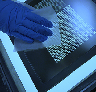
The purpose of a stencil is to allow the transfer of solder paste, conductive adhesive, or other similar material through its aperture openings onto a given substrate (Figure 1). Stencil printing is seen as the lowest-cost process for depositing interconnects for flip-chip packaging; it has been used in the SMT industry at larger geometries for board assembly for many years. There are three main methods for the manufacture of stencils: chemical etching, laser cutting, and electroforming.
 Figure 1. Generic stencil-printing process for flip-chip assembly.
Chemically etched stencils are manufactured using a metal foil (usually brass) that is coated with a film of dry photoresist, then exposed and developed, leaving openings for aperture generation. The stencil is placed in a chemical-etching solution, and the open areas on the metal are etched away. The isotropic nature of the etching step causes an undercutting effect, which inhibits the generation of the fine-web spacing needed for the fine pitch of flip-chip packaging. The web on a stencil is the spacing between the apertures. Chemically etched stencils are not suitable for fine-pitch printing.
Laser-cut stencils are manufactured by mounting a foil onto a frame. A high-powered laser is then driven in a pre-defined manner relative to the layout file to ablate each aperture sequentially into the chosen stencil material. The most common material used in the manufacture of laser-cut stencils is stainless steel; however, nickel is also used because it is said to offer better paste release from the apertures. A polymer foil can also be used as the stencil material. This material gives a cleaner cut compared to metal, and therefore should have smoother inner aperture sidewalls, resulting in better paste release. Recent refinements in the laser-cutting process have been developed to improve the quality of stencil apertures, including smaller laser-spot sizes and water-guided, laser-cutting techniques. One advantage is that the material is pre-tensioned from the framing process prior to cutting. This reduces stencil deformation.
Laser cutting is a sequential process. Therefore, as I/O counts increase on the design, so does the time to manufacture the stencil. This can be a significant disadvantage for wafer-bumping stencils with a high number of apertures because as the number of holes increases, manufacturing time rises to an almost uneconomical point. The heat-melt interaction during the cutting process can create rough inner sidewalls that produce apertures with a larger surface area, and have a tendency to minimize paste release. The heat generated in the cutting process must be controlled so it does not warp the stencil during manufacturing, or damage the fine webs needed for fine-pitch printing. Electro-polished stencils normally are laser-cut stencils that have been smoothed using electrochemical or mechanical polishing methods. However, all metal stencil types can be treated in this manner after manufacturing.
The conventional electroformed-stencil manufacturing process involves taking a conductive mandrel, such as stainless steel, and applying a dry film layer of photoresist to it. This photoresist layer is photo-patterned and developed. The photoresist left on the mandrel after photolithography defines the apertures. The substrate then is placed into an electroplating solution, and a current is applied to the mandrel. The metal normally deposited to create the stencil is nickel or a nickel alloy. Because electroplating is an additive process vs. other subtractive techniques mentioned, deposited metal follows the photoresist mold precisely. After plating, the photoresist remaining in the apertures is removed, and the finished stencil can be framed.
Flip-chip Stencil Requirements
Electroformed stencils are better suited for flip-chip packaging; however, conventional stencil manufacturing techniques are not suited to create foils for sub-150-µm-pitch printing. Advancements using micro-engineering techniques to fabricate enhanced electroformed stencils may enable this.3 To achieve good printing at fine pitch, this technology must be coupled with the latest solder paste materials that contain fine-particle powders (IPC Types 6-8 paste). These stencils have improved aperture quality with micron-tolerance holes, smooth sidewalls for paste release, and thickness uniformity across the foil (Figures 2a and b).
 Figure 2a. 100-µm-diameter aperture.
null
 Figure 2b. 25-µm-thick stencil.
Micron-tolerance apertures are required for fine-pitch printing to ensure consistent paste-printing volume. As an aperture diameter decreases, stencil thickness must also decrease for good paste transfer. An industry rule of thumb states that the stencil should be 2/3 the size of the smallest aperture diameter. For fine-pitch printing, this requires stencil thickness of 75 µm or less. Stencils of this thickness will stretch from the framing process. Therefore, electroformed stencils must be manufactured with a correction factor to enable accurate substrate-to-stencil registration during printing. If not, misprints will occur.
Solder Paste for Flip-chip Packaging
Printing at fine pitch requires a reduction in the particle size distribution (PSD) of the alloy from 20-45 µm (Type 3) to less than 15 µm (Types 6 and 7). To satisfy this criterion, changes in PSD inherently affect solder paste properties. For example, moving from Type 3 to Type 6 PSD increases the number of particles (per unit volume) by about a factor of 15. These finer particles in the solder paste will alter paste rheology (Figures 3a and b). Rheology is the behavior of the paste with regard to flow and deformation. This affects shear stress, strain, and rate. Having the correct rheology is critical for the printing process as it impacts paste roll and aperture fill and release. Flux composition and alloy volume determine paste rheology.
 Figure 3a. 125-µm Type 6 solder paste deposits.
null
 Figure 3b. 90-µm-pitch, Type 7 solder paste deposits.
In addition to WEEE, the RoHS Directive calls for the elimination of lead in electronics. Traditional tin/lead solders must be replaced with lead-free alloys. For stencil printing, the lead-free alloy of choice is the tin/silver/copper (SAC) alloy, which has an increased melting temperature, requiring a change in flux to cope with elevated reflow temperatures and smaller particle sizes.
Printing
With regard to stencil design at fine pitch, it is recommended to round aperture corners because circular apertures are shown to offer better paste release compared to square apertures. Tighter control over the printing setup vs. standard SMT printing is required for fine-pitch printing. The main parameters that must be optimized and controlled are print pressure, print speed, and snap-off. However, additional parameters such as the substrate holder for wafer-level bumping, squeegee selection, environmental control, paste lifetime, and substrate-separation speed are also critical to achieving high yield. As pitches dip below 200 µm, on-board stencil cleaning becomes unsuitable. Therefore, the stencil must be removed from the printer for ultrasonic or pressure-jet cleaning.
Conclusion
If technology and market predictions are correct, the need to consider flip-chip methods of packaging will become more likely and cost-effective as WLP becomes a high-volume, low-cost alternative. More applications will require devices that put increased pressure on the capacities of advanced packaging manufacturers so smaller, faster, and cheaper methods become more sought after. While stencil printing has been used for many years, flip-chip packaging requires further understanding to allow its continued use as the lowest-cost bumping process.
References
- E. Jan Vardaman, TechSearch International, Inc., Austin, Texas.
- John Lau, “Low-cost Flip-chip Technologies.”
- R.W. Kay, E. deGourcuff, I. Roney, N.J. Gorman, “Stencil Printing Technology for Fine-pitch Deposition of Lead-free Flip-chip Interconnects.”
Neil Gorman, technical manager, MicroStencil, may be contacted via e-mail: n.gorman@microstencil.com. Robert Kay, chief technology officer, may be contacted via e-mail: r.w.kay@micro-stencil.com.
Share on:


