


 SMT Prospects and Perspectives: AI Opportunities, Challenges, and Possibilities, Part 1
 Nolan’s Notes: Do More, Get More
 Global Sourcing Spotlight: Don’t Be Afraid of Global Sourcing
STEP 9: Test and Inspection
December 31, 1969 |Estimated reading time: 9 minutes
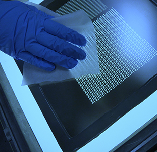
Shipping high-quality products that are free of defects is a challenge that will not disappear. As the industry faces process changes in the transition to lead-free, more test and inspection solutions are needed to meet various requirements.
By Stig Oresjo
Shipping high-quality products free of defects is a challenge that will not diminish as board complexity and cost pressures increase. As the industry faces major process changes in the transition to lead-free manufacturing, more test and inspection solutions are needed to meet varied requirements. Determining the optimal test strategy requires considering a variety of factors such as defect levels, board complexity, defect spectrum, test effectiveness and where defects are introduced in the process. The optimal test strategy for a low-complexity board manufactured in high volumes is different from those of a high-complexity board manufactured in medium to low volumes. For every manufacturing situation, it is important to determine the best balance between the two major test strategies: defect prevention and defect containment. The European regulation for lead-free consumer electronic products will create a significant process change in manufacturing this coming year; and many industry segments that are not mandated to switch to lead-free will do so later. The switch to lead-free will also affect test and inspection. These factors, as well as economic considerations, determine the ultimate test strategy.
Major Drivers
The most important issues for selecting the optimal test strategy are: defect levels; where “defects” are introduced in the manufacturing process; test/inspection effectiveness; and board-dependent issues, such as complexity, production volumes and electrical and visual access.
Defect levels are most often measured as Defects per Million Opportunities (DPMO), also called Parts per Million (PPM). A solder joint is one defect opportunity for defects such as opens, solder bridges, insufficient solder, etc. A component and its placement is also a defect opportunity for defects such as defective, wrong-value and misaligned components. With a production run of 100 PCBAs, in which each board has 10,000 defect opportunities, the entire batch will have one million defect opportunities. If a total of 150 defects are detected on these boards (in all inspection and test steps), this correlates to a DPMO value of 150. An estimation of the yield can be done using the following formula:
Yield = (1 - DPMO/1,000,000)^N
Where DPMO is the DPMO value, and N is number of defect opportunities, let us calculate the yield for a board with 10,000 defect opportunities for DPMO values of 10,100 and 1,000. Corresponding yield numbers are 90%, 37% and 0%. Clearly, the test strategy should be different if the expected raw yield without any test/inspection is expected to be 90% vs. 0%. It is important to know average DPMO values. This should be the average DPMO value for different board types and different days or weeks. It should not be the best number you have achieved over time, and not the “marketing” number you may use. It should be as close to the truth as possible. Typical DPMO values in the industry are between 100 and 1,000. It is also important to have a good understanding of defect types. For example, let’s say that out of all defects, 40% are opens, 30% are bridges, 15% have insufficient solder and 12% are missing components. Before determining the optimal test strategy, one must understand where defects are introduced and can be detected. If, for example, several defects are introduced in the selective wave process, inspection steps prior to this manufacturing step will not be able to detect those. On the other hand, it is an advantage to detect defects early. If the component placement process places a component with a wrong orientation, it is better to detect this prior to the reflow process. This is especially true for expensive components. If these types of defects are caught before reflow, the component can be reused in most cases. After reflow, however, the component must be scrapped.
The last general, board-independent issue is the effectiveness of different test and inspection systems at finding different types of defects. It is recommended that test effectiveness studies are performed with some regularity. A test effectiveness study is performed typically on a small set of boards (about 20 to 100 boards). All defects are categorized into true defects and false calls; process indicators can also be identified. If solder paste inspection (SPI) and AOI pre-reflow are included in the study, potential defects will also be identified. During the test-effectiveness study, no defects should be repaired until the last test/inspection has had a chance to detect all defects.
During the study, accurate recording of each individual defect should be kept. When all boards have been tested and inspected by all systems in the study, a calculation of each system’s test effectiveness can be done. If we assume that a total of 100 defects were identified in the study, and we know that one system found 60 of those 100 defects, then we know the test effectiveness for that system is 60%. We will also have a good understanding of what types of defects different systems can best detect. For example, we might notice that in-circuit test (ICT) is suitable for detecting component defects, while X-ray is good at detecting solder-related defects. In general, these issues typically are independent of board types.
Board-dependent Issues
The optimal test strategy depends on board characteristics. The most important factors are: board complexity; planned production volumes; single-sided vs. double-sided; electrical and visual access; and any specific component issues, such as cost or unknown quality issues. Of these factors, complexity is likely the most important. As board complexity increases, it becomes more challenging to manufacture the board with high yields. The sidebar shows a formula to calculate a complexity index. This formula (or something similar) is recommended. The Complexity Index should be viewed as a rough measure based on easy-to-determine features. It gives an approximate indication of the board’s complexity. The number of defect opportunities (components plus joints) greatly affects the index. If applied to the yield formula used above, the relationship between the number of defect opportunities and yields becomes clear.

A simple example illustrates this point. Let’s assume there are three different board types: one with 100, one with 1,000 and one with 10,000 defect opportunities. If we assume 200 DPMO for all three boards, what would the resulting yield be for each? The board with 100 defect opportunities will result in 98% yield, the board with 1,000 results in 82% and the board with 10,000 results in 14% yield. In this example, the 10,000 defect-opportunity board requires more elaborate test/inspection strategies than the “100” defect opportunity board.
Board volumes play a role in the selecting strategy. For very low volumes, manual or visual inspection and functional test may be enough, especially if the board is low complexity. On the other hand, a high-complexity board in medium- to high-volume production requires test and inspection methods that are automated and have high test coverage. Boards with limited electrical access (including boundary scan) require higher emphasis on automated inspection. If the board has limited visual access, then X-ray test should be emphasized.
Defect Prevention
Defect prevention uses inspection methods to learn about systematic issues in the manufacturing process; and corrective action is taken based on these observations. By reducing systematic defects, significant reduction in defect levels can be achieved. The most suitable place for defect prevention is Design for Manufacturing (DFM), where manufacturing insight is leveraged into board design and layout, resulting in a board that is easy to manufacture with low overall defect levels. The next place for defect prevention is pre-reflow. There are two major reasons for concentrating efforts at this place. First, it is early in the manufacturing process to minimize the number of boards manufactured with defects. Second, the reflow process masks inefficiencies in the paste application and component-placement process.
Analyzing data from test and inspection at the end of the line also allows for some defect-prevention benefits. SPI and pre-reflow AOI can provide valuable information for defect prevention. For example, SPI identifies stencil misalignments at setup, clogged apertures and paste smears. 3-D SPI can also identify paste-volume problems. The root cause of most of these problems can be traced, and corrective actions can be taken. Pre-reflow AOI can detect missing, billboard, wrong-orientation and misaligned components. Orientation problems may be due to a component tray that is placed incorrectly. Adjusting the placement machine often can correct misalignments, billboards and missing components.
Process optimization using defect-prevention techniques works best on high-volume board manufacturing. However, these techniques and philosophies should also be applied to high-mix, low-volume boards.
Defect Containment
With a perfect defect-prevention strategy in place, defect-containment strategies are still required. Studies indicate that many defects are introduced late in the manufacturing process. This is especially true for a wave or selective wave process. For other defects where the root cause is early in the process, detection is possible only after reflow. A good detection-containment strategy is essential to address random and late-introduced defects. Common types are manual/visual inspection (often replaced with post-reflow AOI); automatic X-ray inspection (AXI); electrical process test such as ICT often complemented with boundary scan test; or flying probers for low-volume boards. Some form of functional test is also needed - either powering up the final product, performing hot-mock-up test or board-level functional test. Sometimes this is complemented with some type of burn-in test and/or environmental stress screening (ESS). The overall objective with defect-containment test and inspection is to find as many defects as possible before the product is shipped, minimizing warranty costs and field-failure rates.
There always is an economic consideration in deciding on the amount of test and inspection methods to use, driven by board complexity, board volumes, defect levels and desired quality requirements.
New Challenges: Lead-free
Within a year, many electronics products must comply with lead-free regulations. Today, lead is used in solder paste, components and bare boards. Removing lead in these areas will be a significant process change. From experience, we know that during a process change defect levels typically rise, sometimes significantly. As discussed, increased defect levels mean lower yields and more defects, making test and inspection more important. During the transition, manufacturers may need to implement more test and inspection with higher overall test effectiveness. After defect levels have been reduced to pre-transition levels, test and inspection efforts can be adjusted. We expect large variations from site-to-site and from board type to board type. For some board types, especially lower-complexity boards, insignificant increases in defect levels are expected. However, in cases such as high-complexity boards with many components and different component types, significant defect-level increases are likely. The key is to be ready if defect levels increase.
Economic Decision
Ultimately, the test-strategy decision should be based on economics. The International Electronics Manufacturing Initiative’s (iNEMI) Test Strategy Project developed a good example of a spreadsheet-based economic test-strategy-model tool for comparing test strategies. The model allows inputs for yields or DPMO values out of the manufacturing process, board volumes, board cost, etc., then calculates the total cost of various strategies. The tool is available for free from iNEMI at www.inemi.org/cms/projects/ba/test_strat.html.
Conclusion
Selecting and implementing test and inspection strategies requires analysis of several factors. The optimal solution depends on defect levels, board complexity, manufacturing volumes, different test solutions, test effectiveness and desired quality levels. It is recommended to have both defect-prevention and defect-containment strategies in place.
Stig Oresjo, senior test strategy consultant, Agilent Technologies, may be contacted at (970) 679-3215; e-mail: stig_oresjo@agilent.com.
Share on:


