


 SMT Prospects and Perspectives: AI Opportunities, Challenges, and Possibilities, Part 1
 Nolan’s Notes: Do More, Get More
 Global Sourcing Spotlight: Don’t Be Afraid of Global Sourcing
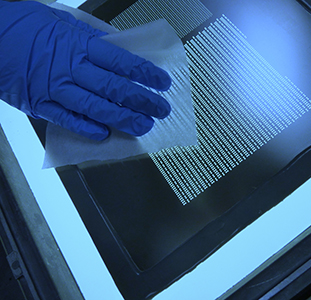
Lead-free Conversion Issues in Component and PWB Surface Finishes
December 31, 1969 |Estimated reading time: 3 minutes
The Massachusetts Lead-free Electronics Consortium, sponsored by the Toxics Use Reduction Institute (TURI) and the University of Massachusetts Lowell, has been working for the last four years to quantify the conversion process to lead-free.
By Sammy Shina and Todd MacFadden
The Consortium is a collaborative effort among companies that represent the entire printed wiring board (PWB) supply chain. The goal of Consortium projects is achieving zero-defect lead-free soldering, while ensuring a level of reliability comparable to that of leaded solder joints. Working with TURI, university researchers and students ran an exhaustive set of experiments to test materials, manufacturing processes and reflow strategies. The research conclusions are unique in visual defect enhancement, and concur with other research activities on high reliability of lead-free joints.
Lead-free conversion testing parameters included material selection (raw PWBs, component finishes, solders and fluxes); process selection (reflow parameters, temperatures and environment); mix of component types and finishes; acceptability (visual inspection); reliability (types and causes); and planning for adverse consequences to conversion. Most component and electronics manufacturing services (EMS) suppliers favor mixing leaded and lead-free components until conversion is completed to avoid duplicate part number costs. The research conclusion of the Consortium is that there is no problem for larger parts such as SOICs, but this can be potentially difficult for smaller footprint components such as QFPs. The Consortium also made decisions regarding which visual tests to perform, what magnification and to what standards, as well as reliability testing including temperature cycling profiles and duration, component pull fixtures, and pulling methodology.
Phase I of testing quantified potential differences in solder alloy combinations and reflow profiles and environments. Phase II tested various PWB surface finishes, three different tin-silver-copper (SAC) solder pastes, and several types of components and finishes, including a mix of SOICs, QFPs and BGAs, as well as tin and palladium-gold component finishes.
Statistical methods were used to investigate different combinations of materials and processes, sample sizes, number and types of leaded baseline samples, and graphical and statistical analysis of data. Novel statistical approaches were used to clarify conclusions, such as multiple range tests, confidence and significance because of the combination of materials and processes examined, which numbered as high as 120.
Reliability results of 2,000 cycles in 0 to 100°C cycling temperature was obtained by pulling component leads at 45° prior and after thermal cycling concurred with prevailing industry knowledge: that SAC alloys perform the best, followed closely by tin-silver, with tin-bismuth lagging behind. All were either equal to or lower than the tin-lead baseline in pull strength. SAC and tin-silver lead-free solders hardened after thermal cycling, while tin-bismuth did not. The PWB surface finish significantly affected the pull test results, with OSP having the highest for SOIC components and SMOC/
HASL performing the best for QFP ones. ENIG finishes yielded the lowest pull strength overall. Other finishes, such as immersion silver and matte tin showed no differences. All other factors such as solder suppliers, reflow profiles and temperatures also showed no difference, either pre- or post-thermal cycling for SOIC components and some differences for QFP ones. Nitrogen was significant for QFPs, but not for SOIC components in reliability testing.
For visual tests, students were trained to use IPC standard 610 for solder joint inspection. Surface finish did not show much difference in visual results: only SMBC/HASL was significantly higher, while ENIG had the lowest visual defects. Reflow profiles and temperatures did not produce significant differences.
Conclusion
These tests show reliable, zero-defect soldering can be achieved with some combinations of solder suppliers, surface finishes and reflow atmospheres. However, there is no drop-in substitute for lead in solder.
Sammy Shina, Ph.D. may be contacted at University of Massachusetts Lowell, (978) 934-2590; E-mail: sammy_shina@uml.edu. Todd MacFadden may be contacted at TURI, University of Massachusetts Lowell, 1 University Ave., Lowell, MA 01834; (978) 934-3391; Fax: (978) 934-3050.
Share on:


