


 SMT Prospects and Perspectives: AI Opportunities, Challenges, and Possibilities, Part 1
 Nolan’s Notes: Do More, Get More
 Global Sourcing Spotlight: Don’t Be Afraid of Global Sourcing
Process Parameters for No-flow Underfills in Flip Chip Construction
December 31, 1969 |Estimated reading time: 12 minutes

Conventional flip chip assembly involves either dispensing a liquid flux on the substrate or dipping the bumps into a thin film of a paste flux before chip placement. The assembly then is reflowed and the die underfilled with an appropriate encapsulant.
By Pericles A. Kondos and Peter Borgesen
No-clean flux residues tend to impair both the wetting and flow of encapsulants as capillary forces draw them between the die and the substrate. These residues are known to have an adverse effect on package reliability. The encapsulant also must be cured, and this hampers throughput.
A no-flow combined flux and underfill, deposited before die placement, not only eliminates reliability issues caused by no-clean flux residues but also may increase throughput by reducing or eliminating encapsulant curing time. Although their performance in thermal cycling tests remains inferior to conventional capillary flow underfills because of the higher coefficient of thermal expansion (CTE) mismatch between a typical no-flow underfill and the solder joints, vendors are making rapid progress. Current offerings show improved performance over conventional underfills that were in widespread use as recently as 2001.
However, several issues must be addressed to create a robust no-flow underfilling process. Careful attention must be paid to underfill dispensing, chip placement and assembly reflow.
- Dispensing must cover the areas where electrical contacts will be made without allowing excessive voids to form in the underfill.
- Chip placement forces must be enough to squeeze out the underfill and permit solder balls to contact the substrate pads.
- The reflow profile must be optimized to reflow the solder balls before beginning to cure the underfill without exposing the underfill to excessive temperatures.
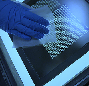
One company's* SMT lab built numerous flip chip assemblies using no-flow underfills from well-known vendors to examine process issues and suggest optimal parameters. Assemblies were cross-sectioned and analyzed for soldering and extrusion using an X-ray microscope, and examined for voiding and delamination from chip and substrate using a scanning acoustic microscope.
Dispensing
The dispense cycle must create a single glob of material of the appropriate volume and shape to allow all bumps to be fluxed during reflow and then form proper fillets. Voids should be few and as small as possible. When designing the dispense process, care should be taken to optimize settings according to encapsulant viscosity. These include the distance of the dispense nozzle from the board. Insufficient clearance tends to prevent the material from exiting the nozzle, and a smaller volume of encapsulant than that calculated will be dispensed onto the board. This problem is more pronounced with high-viscosity materials.
Another viscosity-dependent problem is the tendency of viscous liquids to form a "tail" as the needle retracts. Moving the needle before the tail breaks can deposit encapsulant strings elsewhere on the board. To avoid this, longer retract distances and lower retract speeds must be used for viscous materials; however, this increases cycle time.
The simplest dispense pattern is a single drop at the center of the site. Because the dispense head is not moving, a higher flow rate can speed the process and the tip of the needle can remain a relatively large distance from the substrate. The needle must retract only once at the end of the step. But this pattern is prone to causing assembly voids, and cannot be used at all for large die because the material will not reach the corner bumps.
Other patterns can be programmed, such as an "area fill." This may require the dispense head to trace a long path, but results in better spreading. The dispense head also must be lifted only once at the end of the pattern. Alternatives such as a cross, an "X" or an asterisk might have a shorter total path, but the time savings are compromised when using material that tends to form a tail when the nozzle retracts; therefore, the retract speed must be set to a slow value.
At the same time, an area fill cannot be used with a large die because the material tends to spread too thinly and shrinks back into a more compact shape. It may even break into smaller pieces, virtually guaranteeing large voids.
 Figure 1. Voids under a large die formed because of the dispense pattern.
Other patterns also may form large voids. Figure 1 shows voids appearing under a 550 mil (14 mm) square die. The dispense pattern combined a small area fill with a cross and, finally, an X superimposed with arms extended to the die edge. This pattern produced several void-free assemblies, but occasionally broke, forming large voids. On the other hand, when a single glob of material was dispensed near the center of the site, the material never reached the corner bumps and they failed to solder, even when a larger amount of material was used.
Placement
As the die is placed on the substrate, it first contacts the encapsulant at an area near its center. As it keeps moving downward, it compresses the liquid and pushes it outward. As the liquid moves, it must pass around or over solder bumps, printed circuit board (PCB) traces and other features as it fills the solder mask openings. This motion generates and traps bubbles, especially behind bumps, in a more or less downstream direction.
 Figure 2. Placement bubbles in the encapsulant near the bumps.
Figure 2 shows bubbles near bumps; the die was placed on a glass slide and is viewed from underneath. The image's grainy appearance is caused by solid particles contained within the encapsulant, which dissolved at a higher temperature. The bubbles near the center bumps (arranged in a triangular shape) are comparable in size with the bumps themselves; the size of the bubbles can be estimated by comparing the pitch of the perimeter bumps, which is equal to 10 mil (0.254 mm). The perimeter bumps had similar bubbles, but these were detached and can be seen rising in the fillet (out of focus); one bubble from a corner bump can be seen half under the die and half outside in the lower left corner. Most of the detached bubbles left a much smaller bubble behind them, near the respective bumps. Such behavior is typical of every placement and cannot be avoided. However, component manufacturers may counter bubble formation by minimizing irregularities in the surface of the die and substrate.
Once the material has reached the edges of the die, it must wet the sides and "climb" them to form a fillet. During that time, the die must be held in place because it has a natural tendency to float on the drop of liquid. The danger here is that it may settle later in the wrong place.
The encapsulant's viscosity is the dominant factor in determining the time for which the die must be held in place. Videotaping the liquid as it wetted the sides of the die indicated that the time required for the liquid to stop visibly moving varied from about 0.1 seconds to more than 1 second, depending on the encapsulant.
Not only must the die be held for a certain length of time before the placement head is withdrawn, but it also must be pressed down with a certain force during that time to squeeze out the encapsulant and force it to fill all spaces under the die. Particularly with individual pad openings, the encapsulant must flow through the narrow space between each bump and the opening walls to make space for the bump. However, even when the individual openings are replaced by traces through trenches, allowing freer motion of the encapsulant, a substantial placement force still must be used.
Another important effect of this force is to press the bumps down on the substrate and partially coin them. This brings as many bumps as possible close to their pads before reflow, and helps avoid electrical opens when using no-flow encapsulants. When a conventionally fluxed component is reflowed, the first few bumps to melt and wet their pads exert sufficient force due to surface tension to pull the die downward, since there is no underfill to prevent the die collapsing. This eventually brings all the bumps into contact with the pads, ensuring electrical continuity of the part.
In contrast, reflow encapsulants resist downward motion of the die. This resistance is even higher if the encapsulant has begun to polymerize, which thickens the material appreciably. As a result, ensuring sufficient placement force is essential to bringing as many bumps as possible close to the corresponding pads and generating sufficient force to overcome encapsulant resistance.
The encapsulant also resists lateral motion, and can result in reduced self-centering of the component during reflow. This means accurate placement also is important when using reflow encapsulants.
Force necessary to ensure electrical continuity varies with encapsulant viscosity because more viscous liquids require higher force. For example, a die with 88 bumps and one of the most viscous materials showed consistently good results when a placement force of 800 g was used. But when the force was reduced to 500 g for two dice, both displayed opens. On the other hand, excessive placement force not only risks damaging the die but also bends the substrate, which then bounces when the force is released. This leaves an indeterminate number of bumps coined to a surface that no longer exists, and may even cause the die to move relative to the substrate.
Reflow
Reflow is the most complex procedure to optimize for reflow encapsulants because several processes take place simultaneously and their requirements sometimes conflict. For instance, the material must remain fluid during reflow so it will not prevent joints from forming and the die from collapsing. Yet by the time the board comes out of the reflow oven, it must be substantially, if not completely, cured. Some of these materials are sensitive to variations in the reflow profile, leading to opens if the temperature becomes too high too soon, or even if the heating rate is too high.
Several encapsulants tested require a traditional SMT profile (Figure 3, curve labeled "Standard"). This is an advantage if other surface mount components are to be built at the same time. Additionally, these materials are expected to be the least sensitive to variations in the reflow profile because they are "slow" to start polymerizing. However, they all require a certain amount of post-curing after reflow, typically 30 to 40 minutes.
 Figure 3. The three different types of reflow profiles.
At the other extreme, some encapsulants are not compatible with the "soak" period of traditional reflow. Instead, they respond best when steadily ramped to reflow conditions, and subsequently held for a few minutes at a relatively lower temperature. The post-heat period makes the profile look like a mirror image of the traditional SMT profile (Figure 3, curve labeled "Inverted"). These materials do not require post-cure; essentially the post-curing has been moved inside the reflow oven.
A range of reflow profiles exists between these two extremes, which can be called "intermediate." One such profile is included in Figure 3. These profiles are characterized by a short or absent soak period (occasionally soaking at a lower temperature than usual). No post-cure period exists inside the reflow oven. Some of them require post-curing of various lengths, while others are designed to cure sufficiently during reflow.
 Figure 4. A joint that failed to form because of early onset of encapsulant gelling.
The last two groups of materials start curing faster and, therefore, are more sensitive to reflow profile variations. Figure 4 shows a case where the material started gelling too early, preventing this particular bump from wetting its pad. Bump shape indicates, however, that the other joints have collapsed and the molten solder was pressed onto the pad, trying to form a joint. A thin film of material can be seen separating the bump from its pad. Occasionally, joints formed with these materials have an irregular shape (Figure 5), indicating that the encapsulant began gelling while the solder was still liquid.
 Figure 5. X-ray pictures showing irregularly shaped joints with a 'fast' (no-post-cure) reflow encapsulant.
One question concerning these no-post-cure materials is the effect of the exact profile on the degree of curing. Because the material must cure almost completely in the short interval between the end of collapse and assembly cool down, before it even comes out of the oven, small cool rate variations might affect the degree of curing to a significant extent. This effect will not be discernible when the assembly comes out of reflow, but it will later affect reliability because an insufficiently cured material will be reduced in strength. Encapsulants that use a similar reflow profile but require post-cure should be affected by the cooling rate to a smaller extent.
Voids also can appear and disappear during reflow. When solder joints collapse, material is squeezed still further out and tends to take remaining bubbles behind the perimeter bumps with it. Once these bubbles reach the fillet, they can rise to the surface of the liquid or dissolve in it. As a rule, the fillet comes out of reflow void-free. On the other hand, bubbles under the body of the die or near center bumps cannot reach the fillet during collapse. The only way they can disappear is by dissolving in the liquid encapsulant, and bubbles have been observed to dissolve in a drop of encapsulant held between glass slides. This dissolution is helped by small initial bubble size and elevated temperature, but slows down as the material thickens and stops when it gels or if moisture comes from the substrate and diffuses into the bubbles that still exist.
This behavior shows another advantage of materials requiring a traditional reflow profile. The relatively long soak period at an elevated temperature provides ideal conditions for bubbles to dissolve. A final caveat is to ensure the board is sufficiently dry. If not, new voids will form, even if all the assembly bubbles have dissolved during the earlier stages of the reflow cycle.
Conclusion
With proper board preparation and optimized dispense, placement and reflow conditions, 100 percent electrical continuity can be achieved when using reflow encapsulants without experiencing excessive voids. These will reduce the effectiveness of any underfill. Some materials tolerate only a narrow process window, but others are less sensitive.
With growing understanding of the assembly parameters and ongoing improvements in material technologies, particularly in relation to CTE matching, reflow encapsulants, within their limitations, can replace traditional capillary flow underfills in many cases, simplifying the assembly process and reducing costs.
Pericles A. Kondos, Ph.D., process research engineer, and Peter Borgesen, Ph.D., manager, process research, may be contacted at Universal Instruments Corp., P.O. Box 825, Binghamton, NY 13902-0825. Kondos may be contacted at (607) 779-5136, E-mail: kondos@uic.com., and Borgesen at (607) 779-7343, E-mail: borgesen@uic.com
Share on:


