


 SMT Prospects and Perspectives: AI Opportunities, Challenges, and Possibilities, Part 1
 Nolan’s Notes: Do More, Get More
 Global Sourcing Spotlight: Don’t Be Afraid of Global Sourcing
Step 10: Rework & Repair
December 31, 1969 |Estimated reading time: 7 minutes
By Patrick McCall
In the quest for size reduction, smaller components will become more widespread. With each generation of smaller, more powerful products, new challenges arise when reworking or repairing assemblies. Area arrays present special process considerations when rework and repair is required. These include higher levels of process control, more precise control/application of heat, lead-free solder consideration, and advances in component construction.
The procedure/process for reworking area arrays often is different from reworking standard surface mount components. It is a longer process, with more opportunity for mistakes. The typical procedure includes:
- Removal of old package
- Site preparation
- Component placement
- Flux/paste application
- Heat application
- Inspection.
Removal of Old Package
When removing a failed package, a removal profile may be developed that uses faster ramp rates and shorter times. However, when a device is to be reused, a removal profile similar to the installation profile or the installation profile itself should be used for reflow. This also is the case when dealing with PCBs and packages made from materials that must adhere to strict ramp rate guidelines.
Proper preheating and thorough printed circuit board (PCB) warming is always critical to success. Removing packages by only applying heat from the top can result in damaged or lifted pads. The amount of heat required to bring the solder balls to melting temperature through topical application often will overheat the rework site and exceed recommended heating ramps.
 Figure 1. When using a VOS for alignment, it is desirable to have a fixed location for the component to be picked up by the vacuum nozzle within the reflow head.
null
All solder joints under the package must be liquidus before lifting the package from the PCB. Using rework equipment that uses devices to automatically lift a package after the removal profile is completed are common and generally work well. The removal profile must be validated with thermocouples. If some solder joints do not reach solder melt temperatures and the automated head lifts up, pads will be pulled off the PCB.
It is important to place thermocouples on the outside edges of the array, as well as in the middle, to verify proper, uniform temperatures.
Site Preparation
Once a package has been removed, excess solder on the land patterns usually can be removed using conductive desoldering tools. Other techniques include the use of solder wick or hot gas heating. Temperatures more than 200°C combined with pressure can damage pads or the solder mask.
PCBs with vias through them generally are not good candidates for desoldering tools. While the desoldering tip is moved across the land pattern, the vias can become filled with solder. Attempting to clean out the vias can result in damage to the via, solder mask or PCB. When using solder wick, it is important to place the wick on the PCB and wipe a hot iron tip over the wick. As the solder melts, it will "wick" into the copper braid.
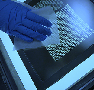
The pads must be clean and free from old solder and flux residue before proceeding with package replacement. When installing micropackages, proper cleaning is as important to the process as the installation profile.
Placement
Placement by hand is a viable option for packages with solder spheres more than 1 mm by using a template or the silkscreen around the land pattern as a guide. A vision overlay system (VOS) can be used to ensure proper alignment. Typically, a minimum magnification of 35X is required.
 Figure 2. To take advantage of the self-aligning properties of array packages, the accuracy of the device that is placed on the PCB must be at least 50 percent.
null
To place CSPs, flip chips and other micropackages successfully, a VOS must be used. A minimum magnification of 70X is required. Placement precision in the Z travel should be 50 µm or less. When placing flip chips, 25 µm is needed. When using a VOS for alignment, it is desirable to have a fixed location for the component to be picked up (Figure 1).
The solder ball must cover at least 50 percent of the pad on the PCB — when the device is placed on the PCB the accuracy must be at least 50 percent to take advantage of the self-aligning properties of array packages (Figure 2). Packages aligned less than 50 percent can migrate one full row of the array.
Flux/Paste Application
Applying the proper amount of flux to the rework site is critical. Too little flux and the solder will not flow correctly; too much and outgassing can occur. Another scenario is that flux will be left over.
Methods for applying flux include using a brush or pen applicator, a piston-driven mechanism to dispense a gel or sticky flux, or a flux "dipping" applicator tool.
Solder paste should be used when solder balls on the bottom of the package are made from 90/10 solder; PCBs have bare copper or gold pads on them; the PCB may be warped; the package contains an elastomer layer for CTE differences; it is critical to have the same joint geometry as the production assembly and solder paste used in initial production; and a specification exists for the joint stand-off height for function or cleaning.
Solder paste can be applied using spot stencils to the PCB, using component stencils to apply solder paste to the component, or using dispensing equipment to apply dots of solder paste to each individual pad. It often is easiest to screen paste onto the component directly and lift the stenciled component off the stencil using the rework unit's pick-up mechanism.
Heat Application
Bottom-side heating is important in soak and reflow phases for successful installation while exposing the PCB and package to a minimal amount of thermal stress.
In the "preheat" phase, bottom-side heating ensures homogenous temperatures across the board. This keeps the PCB from warping, twisting or flexing during the process. Heat application from the bottom of the PCB during the preheat phase also is used to warm the entire PCB.
 Figure 3. During reflow, air or nitrogen passes through the heater and into a nozzle to guide the hot air.
null
During soak, the bottom-side heater should continue operating while heat is added from the top heater. The combination of top- and bottom-side heat application allows the installation site and package to reach a temperature of between 140° and 170°C and stabilize. The stabilization should be maintained for 30 to 60 seconds, allowing the flux to fully activate and driving off volatiles.
During reflow, higher temperatures are applied from both the top and bottom heater. Air or nitrogen passes through the heater and into a nozzle. Often nozzles are vented so the hot air is vented up and away from the PCB and adjacent components (Figure 3). Heat should be applied slowly and evenly.
Lower temperatures should be used when installing micropackages. Because the micropackage essentially is the same size as the silicon die, there is no significant encapsulation for protection. The smaller mass of the solder spheres on the micropackage, coupled with a thin package, allows quick heat transfer through the component. When standard BGAs are installed, heat must be driven through and around the package. Therefore, if a profile for a standard package is used on a micropackage, the component will become super heated.
Usually, a PCB will be populated with thermocouples in various locations. When developing a profile, thermocouples should be placed on top of the device and on at least one solder ball and the bottom side of the PCB, both directly under the rework site and away from the rework site.
Positioning thermocouples in these locations allows monitoring of temperature variations between the parts of the package and monitoring of the thermal environment to which the solder balls are exposed.
PCBs can be subjected to too much heat, as can packages. This can cause damage to circuitry and microvias, as well as PCB delamination. The thermocouple on the bottom of the PCB away from the rework site ensures the entire board is warmed properly.
If using a site with a package already installed, thermocouples must have contact with the existing solder joints. This is best accomplished by drilling through the bottom of the board into a solder joint and affixing the thermocouple with an epoxy/adhesive or other means to secure it.
When developing profiles through an actual installation, the solder balls must touch the thermocouples throughout the entire process. Once a profile has been defined, it is key to rerun the profile with the determined parameters in a non-changing environment.
Inspection
The installed package should be inspected. For area-array packages, X-ray systems are the most common method, followed by video microscopes that look under the component at a 90° angle. After visual inspection, electrical testing often verifies installation.
Once defects are identified, improvements must be made to the inspection process.
Patrick McCall, senior product manager, may be contacted at PACE Inc., 9030 Junction Drive, Annapolis Junction, MD 20701, (301) 497-8837; Fax (301) 490-0193; E-mail: pmccall@paceworldwide.com.
Share on:


