


 SMT Prospects and Perspectives: AI Opportunities, Challenges, and Possibilities, Part 1
 Nolan’s Notes: Do More, Get More
 Global Sourcing Spotlight: Don’t Be Afraid of Global Sourcing
Automated AMI Analysis of Components Prior to Board Assembly
December 31, 1969 |Estimated reading time: 6 minutes
When a semiconductor component fails in service or during testing, the mechanism of failure may be related to an anomaly within the chip circuitry or in the package surrounding the chip.
By Tom Adams
Anomalies related to chip design, lithography or materials often are revealed by various types of electrical testing before assembly. Packaging-related failures, however, may be caused by a packaging anomaly that remains undetected until it leads to an electrical failure.
The cause of a packaging-related component failure may be a delamination, void, crack or other anomaly at a critical location in the package architecture. In many production sequences, the package itself is the item least likely to be tested for anomalies. Automatic test equipment (ATE) and other electrical tests identify many chip-level defects, while automated optical inspection (AOI), in-circuit test (ICT) and other tests during assembly identify both electrical and component placement defects. At the same time, an internal packaging defect is likely to go unnoticed unless it happens to produce an early electrical anomaly.
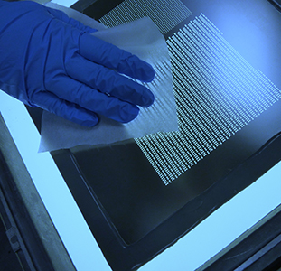
In some production lines, automated acoustic micro imaging (AMI) is used to detect anomalies in packaged components before board assembly. The components are carried in JEDEC-style trays or strips. An entire tray is imaged at one time to find internal packaging defects in the components. The process adds effort and cost to production, but ensures that only those components free from internal packaging defects will be used in board assembly.
When automated AMI first was introduced, it was thought that it would find application only in the low-volume production of systems with high overall value. This has turned out not to be the case. Although some automated AMI work is carried out in low-volume production of expensive items, it also is used in high-volume production, either as batch sampling to gauge the overall rate of package defects, or as 100 percent inspection of critical components. It has been used in instances where the need for rapid assembly has required the use of components from non-qualified sources. On some occasions, negotiations have taken place between suppliers and assemblers to determine which will apply automated AMI to ensure packaging integrity.
Several forms of AMI systems exist. Laboratory-based C-SAM systems, whose primary function is the analysis of individual components, also can perform automated acoustic inspection of groups of components and of individual trays, and are sometimes used for low-volume production. Fully automated systems (FACTS2) use the same imaging technology, but are designed for much higher throughput as a screening tool.
An automated AMI system feeds trays of components into the acoustic imaging area without a technician. The tray itself is raster-scanned as though it were a single component having a huge surface area; that is, the ultrasonic transducer (or scan head) does not pause to raster-scan each component individually. Depending on the component arrangement in the tray, the scanning pattern can be modified to skip "blank" areas like the spaces between rows of components, thus achieving faster scanning.
The ultrasonic transducer uses ultrasound at a selected frequency between 10 and 300 MHz. The thinness of most packages makes it possible to select higher frequencies that yield higher spatial resolution in the acoustic image of the tray. The actual resolution, however, is controlled by user choice, subject to the material properties of the device under test, and varies from one application to another. For a given package type, the user may be interested only in internal defects above a given size. In this case, lower resolution will suffice. A different package may require very high resolution because even tiny delaminations or voids can result in failures in this package. Using sufficiently high resolution permits zooming in on a portion of the tray image to see details in the image of a single component. Used in this way, the images serve not only for component screening but also for component failure analysis.
As the ultrasonic transducer raster-scans the tray of components, it continually pulses ultrasound into the components and receives the return echoes from the interior of each component. The pulsed ultrasound is reflected by material interfaces in the component — for example, the interface between the molding compound and the die face, or between the die and the die-attach material. Interfaces between solid materials such as these return echoes that have amplitudes that, while covering a wide range, can be described as moderate. Internal anomalies such as voids, delaminations and cracks contain air, which is a gas; these anomalies return echoes of much higher amplitude.
This difference in amplitude makes AMI a powerful tool for identifying internal defects, which are conventionally visualized as red in pseudocolor AMI images. The difference in amplitude also makes it possible to use software to automatically identify and remove individual components that fall within the user-identified "defect" classification because they have internal delaminations or other anomalies above a given size or at a critical location.
Echo signals arrive at the transducer from different depths within a component at slightly different times. Because the user often knows which particular internal feature or interface (the die face, for example) is most likely to harbor a defect, the program may gate the signals by using a time window that processes only echoes from that depth. Thus, a user may understand that a given component is most likely to have die face delaminations that eventually can shear off wires. The user can program the automated AMI system to look specifically at this depth.
The user also can program the system to gate on more than one depth — a useful technique when internal defects may be anticipated at the die attach as well as the die face. If the component architecture is complex, it may be more fruitful to use an alternate method that uses through-transmission ultrasound rather than reflection-mode ultrasound. With this method, a sensor beneath the tray reads ultrasound that has been pulsed by the raster-scanning transducer and that has traveled through the entire thickness of the component. The advantage of this method is that it identifies defects in all depths of the component.
 Figure 1. Automatically generated acoustic image of a tray of 40 PQFPs. This tray was imaged using a 50 MHz ultrasonic transducer at high resolution. Red areas are defects. Software identifies defective components and can feed data to factory information systems.
null
In Figure 1, seven of the components have obvious delaminations (red) of the die face from the molding compound. The return echo signals were gated broadly to include the die face depth. In five of the components, the die face is completely delaminated. Even though this defect is conspicuous acoustically, these components could pass electrical tests easily; that is, the delamination of the molding compound from the die might require many hours of use before the delamination reaches and breaks wires. Acoustic imaging of this component after system failure probably would show the same delamination, but post-failure examination would not reveal that the delamination existed at the time of board assembly.
 Figure 2. Low resolution may be sufficient for effective screening. High resolution (above) permits enlargement of individual components. The die face delamination (red) also extends vertically as a crack (arrow).
null
Figure 2 is an enlargement (possible because of the high resolution used in scanning) of one of the defective components in the tray in Figure 1. In addition to total delamination at the die face, there is a separate curved feature near the right end of the die. This feature is a vertical crack extending upward into the encapsulant and actually is an extension of the die face delamination. A second package in this tray had a similar defect, as did several packages in other trays.

null
Conclusion
Tray-based automated AMI primarily is a screening process, but in many instances also can provide failure analysis and process control information. It is used with numerous plastic package types, and for other critical items such as bonded wafers and ceramic chip capacitors. The goal in all cases is the same: to achieve board assembly with only defect-free components.
Tom Adams, consultant, may be contacted at Sonoscan Inc., 2149 E. Pratt Blvd., Elk Grove Village, IL 60007; (847) 437-6400; Fax: (847) 437-1550; E-mail: info@sonoscan.com; Web site: www.sonoscan.com.
Share on:


