


 SMT Prospects and Perspectives: AI Opportunities, Challenges, and Possibilities, Part 1
 Nolan’s Notes: Do More, Get More
 Global Sourcing Spotlight: Don’t Be Afraid of Global Sourcing
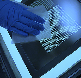
Electroless Ni/Electroless Pd/Immersion Au/Electroless Au (ENEPIGEG) Plating Process For Gold Wire Bonding on Organic Package Substrates
September 21, 2010 |Estimated reading time: 14 minutes
Abstract
This study examines the wire bonding reliability of electroless gold plating after heat treatment. The results indicate that in the electroless Ni/immersion Au/electroless Au (ENIGEG) plating process, the electroless Ni (EN) under the immersion Au/electroless Au (IGEG) diffused onto the surface of the gold plating by heat treatment and changed to nickel oxide, resulting in the prevention of wire bonding between the gold wire and the gold plating and a decrease in the bonding strength. For restraining the diffusion of underplated nickel onto the surface of the gold plating, it was found that the application of electroless Pd (EP) between the underplated nickel and the gold plating is effective. It was concluded that the wire bonding reliability of ENEPIGEG after heat treatment was equivalent to that of conventional electrolytic Au plating on electrolytic Ni plating.
To investigate other causes for low wire bonding reliability in ENIGEG, bonding strengths resulting from combinations of electrolytic and electroless processes were evaluated. A noteworthy result was that the bonding strength of electrolytic Ni (SB-Watt)/IGEG was remarkably better than that of EN/Electrolytic Au after heat treatment. The wire bonding reliability of electroless Au deposit (IGEG) was excellent on electrolytic Ni (SB-Watt); however, it was poor on electroless Ni. It was found that the grain size of the electroless gold deposit coordinated with the grain size of the underplated Ni deposit with the growth of the epitaxial crystal. The large grain size of the gold deposit decreased the grain boundary of the gold deposit and reduced the grain boundary diffusion from the underplated metals onto the gold plating. In the gold wire bonding, the large gold grain improved the bonding strength by reducing the contaminations accumulating at the gold grain boundary of the interface between the gold plating and the gold wire. It was concluded that the wire bonding reliability after heat treatment depended on the diffusion behavior of the underplated metals and the grain size of the gold deposit.Introduction Since portable electronics are becoming increasingly popular, the numbers of chip size packages (CSPs) and ball grid arrays (BGAs) used for semiconductor packages mounted on high-density PCBs are increasing. As shown in Figure 1, semiconductor chips and package substrates are connected by gold wire bonding in most CSPs and BGAs, and printed wiring boards and package substrates are connected by solder balls. To satisfy the reliability of these connections, it is essential to gold- plate the terminal surfaces on both sides of the package substrate. The mature technology of electrolytic gold (E'lytic Au) plating has been traditionally used for surface finishing of package substrates. Today, electroless gold (EG) plating technology, which does not require the use of lead for electrolytic plating, is becoming the focus of interest due to an increase in speed and consistent advances in substrate circuit integration [1].
Electroless gold plating technology, however, does have some technical problems, the most immediate of which relate to wire bonding. This bonding is the process of connecting semiconductor chips and package substrates with gold wire by a thermal ultrasonic (thermosonic) bonding process. The heat history during the process of semiconductor packaging causes a reduction in the pull strength of wire bonding by contaminating the plated surfaces [2]. Figure 1: Structure of the electronics package (wire bonding type).
Therefore, the causes for and the possibility of improving the low pull strength of wire bonding on electroless gold plating surfaces after heat treatment are studied here. Our findings in these areas indicate that the lowered pull strength of wire bonding was due to the contamination of the gold-plated surface by the diffusion of nickel plated under electroless gold plating [3]. This paper discusses the newly-developed multi-layer ENEPIGEG as a process for improving low pull strength, and the variations in gold grain size with combinations of electrolytic and electroless plating processes as a root cause of low wire bonding reliability.Experiments Sample Preparation for Wire Bonding
The test substrate for gold wire bonding was made of an epoxy resin copper clad laminated board consisting of 25 tm thick copper foil and a woven glass fabric base material. Acid degreasing, micro etching and acid rinsing were used as pretreatments for the gold plating process for the test substrates. After this pretreatment, the gold plating processes listed in Table 1 were applied. The following electroless processes were used: Immersion Pd plating (activation), electroless Ni plating (EN) with hypophosphate as the reducing agent, electroless pure Pd plating (EP) with formate as the reducing agent, cyanide-type immersion gold plating (IG) and non-cyanide-type electroless gold plating (EG). For the electrolytic processes, a semi-bright Watt bath (sulfate bath), a bright Watt bath and a bright sulfamate bath for electrolytic nickel plating were used in order to change the nickel grain size after the pretreatment. Cyanide-type electrolytic strike gold and cyanide-type electrolytic gold with thallium ion as a grain refiner were used after nickel plating. Nine gold plating combinations were evaluated by electrolytic and electroless processes, as shown in Table 1. Table 1: Gold plating combination with electroless and electrolytic process.Wire Bonding evaluation Method
Wire bonding was performed using Shinkawa UTC-230BI under the following conditions: gold wire with a diameter of 28 jtm, plate temperature of 150°C, a load of 100 g and an ultrasonic output of 120 PLS applied for 20 ms. The wire pull strength was measured using a Dage 4000 all-purpose bond tester.Results and Discussion Wire Bonding Reliability of Electroless Ni/Pd/Au Plating
(1) Degradation of Wire Bonding Strength by Thermal Treatment
Figure 2 shows the relationship between the heat treatment conditions and the pull strength of wire bonding. For gold plating, the pull strength of wire bonding before heat treatment on the electroless gold (ENIGEG) was similar to that of the electrolytic gold (E'lytic Ni (SB-Watt)/E'lytic Au). However, when the heat treatment was continued, the pull strength of wire bonding of the electroless gold decreased and/or misbonding occurred. On the other hand, the wire bonding reliability of the electrolytic gold almost retained constant pull strength independent of the heat treatment. Figure 2: Wire bonding reliability of gold plating.Therefore, the cause for the decrease in the pull strength with heat treatment was studied. The electroless gold-plated surface was examined by XPS (X-ray photoelectron spectroscopy) after heat treatment in order to analyze the cause for the decrease in the pull strength of wire bonding. Results of the examination are shown in Figure 3. It was observed that the underplated nickel moved over to the gold-plated surface to form nickel oxide. To determine the depth profiles of nickel in the gold layer, the surface near Ar sputtering was also analyzed by XPS. Figure 4 shows that nickel oxide was concentrated on the gold surface. The distribution of Ni on the gold surface was also observed by AES (Auger electron spectroscopy). The result shown in Figure 5 suggests that nickel diffusion occurred through the grain boundary of the gold layer. From these findings, it was concluded that the decreasing pull strength was caused by the diffusion of underplated nickel by the heat treatment, which occurred through the grain boundary of the gold layer. The accumulation of nickel diffusion at the grain boundary on the gold surface seems to prevent the bonding of the gold wire by thermal ultrasonic mode.
(2) Improvement in the Pull Strength of Wire Bonding After Heat Treatment
Two methods for controlling the formation of nickel oxide over the gold-plated surface that decreases the pull strength of wire bonding were studied. The first method was to increase the thickness of the electroless gold-plated layer. Figure 3: XPS analytical results of electroless plated gold after heat treatment (surface profile).Although this method was effective, its main disadvantage was the increase in cost.
The second method was to suppress nickel diffusion by generating an electroless plated layer that was stable against oxidation as the intermediate layer between the underplated nickel layer and the gold-plated layer.
(3) Selection of the Electroless Plating Intermediate Layer
A comparative study on the different materials used to form the intermediate layer between the gold- and the nickel-plating layers was conducted using the oxidation-reduction potential as the reference index, since oxidation plays a significant role in nickel diffusion to the gold surface. As a result, electroless palladium plating was selected, since it is difficult to oxidize, usable as the bonding layer for gold wire and adaptable to electroless plating. Figure 4: XPS analytical results of electroless plated gold after heat treatment (depth profile).
 Figure 5: Nickel distribution over gold plating surface with AES analysis.(4) The Restrictive Capacity of electroless Palladium Plating Against Nickel Diffusion
The Ni/Au ratio was analyzed by XPS, varying the thickness of the intermediate palladium layer of the Ni/Pd/Au plating to confirm the reliability to restrict nickel diffusion. As shown in Figure 6, the nickel diffusion drastically decreased when the thickness of the electroless palladium plating, as a barrier metal, was 0.05 tm or more.
(5) Wire Bonding Reliability of Electroless Ni/Pd/Au The terminal surface was first plated with 5 tm of electroless Ni (EN). Then, using the electroless plating method, an intermediate palladium layer (EP) with a thickness of 0.5 tm was deposited, followed by a gold layer (IGEG) with a thickness of 0.5 jtm. Samples obtained in this way were treated at 150°C for 50 hours to measure the pull strength of the wire bonding. It was confirmed that a high level of wire bonding pull strength is attainable by electroless Ni/Pd/Au plating, even after heat treatment, as shown in Figure 7. The wire bonding reliability of the electroless multi-layer Ni/Pd/Au plating (ENEPIGEG) was equivalent to that of the electrolytic Ni/Au plating (E'lytic Ni (SB-Watt)/E'lytic Au). Figure 6: Thermal diffusion barrier of electroless Pd.
 Figure 7: Wire bonding reliability of electroless Ni/Pd/Au.Wire Bonding Reliability of Gold Plating Combined with Electrolytic and Electroless Processes
(1) Combinations of electrolytic and electroless processes Nine typical combinations of electrolytic and electroless process plating techniques for nickel, palladium and gold were applied and evaluated. These combinations are shown in Table 1. ENIGEG, ENEPIGEG and Ni (SB-Watt)/E'lytic Au were tested in previous evaluations. The wire bonding reliability of E'lytic Ni/IGEG and EN/E'lytic Au were evaluated in this study for the first time.
(2) Wire bonding reliability of the combined gold plating processes
The wire bonding reliability of the gold plating combinations are shown in Figure 8. After heat treatment, excellent reliability was found in the following groups: ENEPIGEG [4, 5], Ni (SB-Watt)/E'lytic Au and Ni (SB-Watt) /IGEG. Poor reliability was found in ENEPIG [6], ENIGEG, Ni (B-Watt)/E'lytic Au, Ni (SB-Sulf.)/E'lytic Au and EN /E'lytic Au. The worst reliability was brought by Cu/E'lytic Au, which is the direct electrolytic gold plating process used on flexible printed circuit boards.
(3) Surface morphology and cross sectionThe surface morphology was observed by SEM and the cross section was observed by FIB/SIM. The results are shown in Figures 9, 10 and 11. Figure 8: Wire bonding reliability of the Au plating combination with electroless and electrolytic process.
Figure 9: Surface Morphology and FIB/SIM Cross Section of the Au plating combination with electroless and electrolytic process.
Figure 10: Surface Morphology and FIB/SIM Cross Section of the Au plating combination with electroless and electrolytic process.
Figure 11: Surface Morphology and FIB/SIM Cross Section of the Au plating combination with electroless and electrolytic process.
There were significant differences in the gold grain sizes on the gold plating combinations. The number of grain boundaries in each gold plating process was measured, and the relative density of the gold grain was calculated by squaring the number of the grain boundaries. To compare the size of gold grain size of each process, the obtained values of the relative density of gold grain are shown in the photographs of Figures 9, 10 and 11.
The groups containing larger gold grains were Ni (SB-Watt) /E'lytic Au, Ni (SB-Watt)/IGEG and Cu/E'lytic Au, followed by ENEPIGEG. The groups containing middle sized gold grains were ENIGEG, Ni (B-Watt)/E'lytic Au, Ni (SB-Sulf.)/E'lytic Au and EN/E'lytic Au. ENEPIG had the smallest gold grain among all of the gold plating processes.
The gold grain became large by arranged with the large nickel grain, the large palladium and the large copper grain. The grain size of the gold deposit coordinated with the grain size of underplated Ni, Pd and Cu, as the epitaxial crystal growth. The grain size of the electroless Ni was the smallest in the Ni plating processes because of the amorphous nickel-phosphorous deposit (Ni-P). The grain size of the electroless gold (IGEG) was dependent on the thickness of the gold layer. The gold grain of ENEPIGEG was larger than that of ENEPIG. In electrolytic Ni plating, the degree of brightness affected the grain size of the electrolytic Ni deposit; the grain size of bright Ni was smaller than that of semi-bright Ni [7].
(4) Diffusion of underplated metal onto Au surface
The diffusion behavior of underplated metal is important for gold wire bonding, as described in the evaluation of electroless Ni/Pd/Au. Electroless Pd provided an excellent barrier from Ni diffusion onto the Au surface. The diffusion behavior of the gold plating combinations was evaluated and the results are shown in Table 2. Ni diffusion did not occur in ENEPIGEG and ENEPIG. The groups in which there was little Ni diffusion included Ni (SB-Watt)/E'lytic Au and Ni (SB-Watt)/IGEG. Pd diffusion occurred in ENEPIG for the thin immersion gold layer, but did not occur in ENEPIGEG for the thick electroless gold layer. The groups in which a great deal of Ni diffusion occurred include ENIGEG, Ni (B-Watt)/E'lytic Au, Ni (B-Sulf.) /E'lytic Au and EN/E'lytic Au. A large amount of Cu diffusion occurred in Cu/E'lytic Au.The textbook of wire bonding [8] describes the diffusion behavior of metals, such as Ni, Pd and Cu, through gold films. Ni diffuses rapidly through the gold grain boundary and is oxidized on the gold surface. Pd diffuses fastest through the gold grain boundary but is not oxidized. Cu diffuses fastest through the gold grain or gold crystals as bulk diffusion, and is oxidized.
(5) Wire bonding reliability ranking of Au plating
The wire bonding reliability depends on the gold grain size and the diffusion barrier effect of the metal through the gold plating. The groups that exhibited excellent reliability included ENEPIGEG, Ni (SB-Watt)/E'lytic Au and Ni (SB-Watt)/IGEG. These groups had larger gold grains and little or no Ni grain boundary diffusion. The small amount of Ni contamination did not affect the wire bonding reliability when the gold grain was large. The other gold plating processes showed the poor wire bonding reliability. These gold plating processes had smaller gold grains, a great deal of Ni grain boundary diffusion, Pd grain boundary diffusion or Cu bulk diffusion. The application of a thick EG in ENEPIG is required for the improvement of reliability by enlarging the gold grain and reducing the Pd grain boundary diffusion.
In gold wire bonding, the large gold grain improved the wire bonding strength by reducing accumulated contaminations at the gold grain boundary of the bonding interface between the gold plating and the gold wire. It was concluded that large grain size of the gold deposit and less Ni, Pd and Cu diffusion were essential for excellent wire bonding reliability after heat treatment. Table 2: Under-plated metal diffusion onto gold surface by heat treatment at 150°C (Atomic %).ConclusionsThe wire bonding reliability of electroless gold plating and combinations of electrolytic and the electroless plating after heat treatment were examined. After heat treatment, nickel under the gold plating diffused onto the gold surface and changed to nickel oxide, resulting in the prevention of wire bonding between the gold wire and the gold plating and a decrease in bonding strength. In this study, it was found that the application of electroless palladium plating between the underplated nickel and the gold plating is effective for restraining underplated nickel diffusion onto the surface of the gold plating.The grain size of the gold plating coordinated with the grain size of the metals under the gold plating as the epitaxial crystal growth. The large grain of the gold plating decreased the grain boundary of the gold plating and reduced the grain boundary diffusion of the underplated metals through the gold plating layer. Large gold grains improved the wire bonding reliability by the reduction of grain boundary diffusion. However, the large gold grains in Cu/E'lytic Au were not effective due to Cu bulk diffusion. It was concluded that the wire bonding reliability after heat treatment of ENEPIGEG and E'lytic Ni/IGEG was equivalent to that of conventional E'lytic Ni (SB-Watt) /E'lytic Au and that the wire bonding reliability depended on the diffusion behavior of the underplated metals and the grain size of the gold deposit.
References: 1.H. Yue and M. Lamson, "Effect of Plating Stubs of BGA Packages on Spurious EM Radiation," Proc. 50th Electronic Components & Technology Conference, Las Vegas, Nevada, 2000, p. 786.2. R. W. Johnson, M. Palmer, M. J. Bozack and T. Isaac-Smith, "Thermosonic Gold Wire Bonding to Laminate Substrates with Palladium Surface Finishes," IEEE Transactions on Electronics Packaging Manufacturing, vol. 22, 1999, p. 7.3. K. Hasegawa, A. Takahashi and A. Nakaso, "Electroless Gold Plating For Semiconductor Package Substrate," Proc. 1st IEMT/IMC Ohmiya Japan, 1997, p. 230.4. J. Joshi and S. Greiner, "Wirebondability of Electroless Ni/Au Plated Semiconductor Package Substrates," Proc. IMAPS 2002 Denver, Colorado, IMAPS, 2002.5. K. Hasegawa, A. Takahashi, T. Noudou and A. Nakaso, "Electroless Ni/Pd/Au Plating for Semiconductor Package Substrate," Plating & Surface Finishing, Vol. 91(11), 2004, p. 20.6. K. Johal, S. Lamprecht and H. Roberts, "Electroless Nickel/Electroless Palladium/Immersion Gold Plating Process for Gold and Aluminum-Wire Bonding Designed for High-Temperature Applications," Proc. 2004 SMTA Pan Pacific Symposium, Oahu, Hawaii, SMTA, 2004.7. M. Eshelman, R. Huemoeller, F. Cordes and D.T. Brown, "Substrate Plating Factors Necessary for High Quality Wire Bonding on BGA," Proc. SEMICON WEST 1999 San Francisco, California, IEEE, 1999.8. G. Herman, Wire Bonding in Microelectronics, Chapter 6, Published by McGraw-Hill, New York, 1997.As originally published in the proceedings of SMTA International, October 4-7, 2009.Access thousands of full-length technical articles at the SMTA Knowledge Base.Don't miss the September issue of SMT Magazine! Find it here.
Share on:


