


 SMT Prospects and Perspectives: AI Opportunities, Challenges, and Possibilities, Part 1
 Nolan’s Notes: Do More, Get More
 Global Sourcing Spotlight: Don’t Be Afraid of Global Sourcing
MIRTEC to Preview SiP Inspection and Measurement at SEMICON West
June 11, 2015 | MirtecEstimated reading time: 2 minutes
MIRTEC, "The Global Leader in Inspection Technology," will exhibit its most recent solutions for System in Package (SiP) inspection and measurement at SEMICON WEST 2015; July 14-16, 2015, at the Moscone Center in San Francisco, California. Visitors are invited to booth # 2343 for a detailed demonstration of this exciting new technology.
Brian D’Amico president of MIRTEC’s North American Sales and Service Division stated; “The growing demand for miniaturization and higher functionality at reduced production costs has led to the industry requirement of System in Package (SiP) solutions. An SiP is a number of integrated circuits enclosed in a single package. The SiP performs all or most of the functions of an electronic system. These packages are typically used in mobile devices such as cell phones and digital music players. Dies containing integrated circuits may be stacked vertically on a substrate and are internally connected by wire bond to the package. Alternatively, with a flip chip technology, solder bumps are used to join stacked chips together. As one can imagine, this complex arrangement of advanced packaging presents a challenge to the inspection environment.”
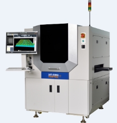
MIRTEC’s MP-520 system was developed specifically to address the challenges related to SiP inspection. The MP-520 combines Precision Linear Drive Motor Technology with MIRTEC’s exclusive 25 Mega Pixel CoaXPress Camera System, a 3D Confocal Measurement system and revolutionary OMNI-VISION 3D Digital Multi-Frequency Moiré Technology to provide high-speed, high-resolution inspection and measurement for SiP and other semiconductor applications. The MP-520 also is configured with eight (music) phase color lighting and four (4) 10 Mega Pixel side-view cameras.
[10:32:14 PM] Beb: The MP-520 is suitable for measurement and inspection of the following manufacturing criteria:
- Solder Ball/Bump – Presence, Pitch, Offset, Height, Co-Planarity and Bridging
- Bond Wire - Short, Broken, Shift and Loop Height
- Chip Bond - Offset, Height, Crack and Chip
- Discrete Device – Presence, Offset, Height, Co-Planarity and Solder Fillet
- Heat Sink - Presence, Offset and Height
- Under-Fill – Presence, Fillet and Height
- PCB - Scratch, Contamination and Bridging
- Package - Warpage, Crack, Marking, Dimensions and Chipping
Inspection and measurement results are stored in a central database, enabling customers to remotely access SPC data through MIRTEC’s INTELLISYS total quality management system software. This software suite promotes continuous process improvement by allowing the manufacturers to track and eliminate defects on inspected assemblies. INTELLISYS also provides remote debugging and monitoring of up to eight production lines, allowing MIRTEC customers to further maximize the efficiency of the inspection process.
“MIRTEC has gained a solid reputation in the semiconductor inspection industry by providing unprecedented performance, quality and cost-effectiveness to the manufacturing environment,” continued D’Amico, “We have achieved a high level of customer satisfaction with a growing number of global semiconductor companies for our advanced back-end inspection solutions. We look forward to welcoming visitors to our booth # 2343 during the three-day event.”
Share on:


Suggested Items
Taiyo Circuit Automation Installs New DP3500 into Fuba Printed Circuits, Tunisia
04/25/2024 | Taiyo Circuit AutomationTaiyo Circuit Automation are proud to be partnered with Fuba Printed Circuits, Tunisia part of the OneTech Group of companies, a leading printed circuit board manufacturer based out of Bizerte, Tunisia. on their first installation of Taiyo Circuit Automation DP3500 coater.
Vicor Power Orders Hentec Industries/RPS Automation Pulsar Solderability Testing System
04/24/2024 | Hentec Industries/RPS AutomationHentec Industries/RPS Automation, a leading manufacturer of selective soldering, lead tinning and solderability test equipment, is pleased to announce that Vicor Power has finalized the purchase of a Pulsar solderability testing system.
AIM Solder’s Dillon Zhu to Present on Ultraminiature Soldering at SMTA China East
04/22/2024 | AIMAIM Solder, a leading global manufacturer of solder assembly materials for the electronics industry, is pleased to announce that Dillon Zhu will present on the topic: Ultraminiature Soldering: Techniques, Technologies, and Standards at SMTA China East. This event is being held at the Shanghai World Expo Exhibition & Convention Center from April 24-25.
AIM to Highlight NC259FPA Ultrafine No Clean Solder Paste at SMTA Wisconsin Expo & Tech Forum
04/18/2024 | AIMAIM Solder, a leading global manufacturer of solder assembly materials for the electronics industry, is pleased to announce its participation in the upcoming SMTA Wisconsin Expo & Tech Forum taking place on May 7 at the Four Points by Sheraton | Milwaukee Airport, in Milwaukee, Wisconsin.
Hentec/RPS Publishes an Essential Guide to Selective Soldering Processing Tech Paper
04/17/2024 | Hentec Industries/RPS AutomationHentec Industries/RPS Automation, a leading manufacturer of selective soldering, lead tinning and solderability test equipment, announces that it has published a technical paper describing the critical process parameters that need to be optimized to ensure optimal results and guarantee the utmost in end-product quality.