


 SMT Prospects and Perspectives: AI Opportunities, Challenges, and Possibilities, Part 1
 Nolan’s Notes: Do More, Get More
 Global Sourcing Spotlight: Don’t Be Afraid of Global Sourcing
No Time for a Board Spin? Selective Solder Mask Removal
January 6, 2016 | Bob Wettermann, BEST Inc.Estimated reading time: 2 minutes
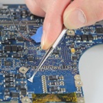
What do you do when you need solder mask removed quickly? What do you do when you get the boards back from the shop and there’s a missing pad, or your design team did not catch the design error in the pad or trace area, resulting in mask where it’s not supposed to be? Perhaps the test group tells you the RF shields need to have the trace opened up in order to pass the testing, but there are literally thousands of boards in the supply chain needing this modification. In these cases solder mask needs to be removed—usually in a hurry—in order to fix these problems.
Outside of re-spinning the board and starting over, there are several processes that can selectively remove solder mask in a controlled and consistent fashion. Some are better controlled than others and include mechanical abrasion, chemical etching, and micro and laser ablation.
Several factors will help determine the method to use including the type of solder mask, and where the area of interest is located. Other factors are the quantity of PCBs, the amount of solder mask needing removal and whether the circuit boards are bare boards or are populated with components.
Grinding and Scraping
One of the most straightforward methods of mask removal is via scraping or grinding of the soldermask. Since solder mask is only a little more than 1mil in thickness it does not require a large mechanical force to scrape it off. With either the use of a knife, scraper, pick or eraser, thin layers of mask can be removed by a skilled and certified repair technician. A multitude of equipment rework stations containing drills, grinders, rotating brushes, and the like are commercially available that the rework technician can use.
There are several drawbacks to this process, namely operator fatigue on large projects, and the lack of repeatability when ultra fine dimensional requirements need to be adhered to. Even with steady hands and fabricated masks the tolerances that can be held by skilled personnel is to ±10 mils. In addition, the depth control using this technique is very poor and underlying laminate or copper layers may be damaged as there is a lack of depth control. The positive aspects of this method are that no special set-up is required and it can be done by almost anyone for prototype or low-volume rework.
Another method that can control the depth of the cut is through the use of a milling machine to remove the solder mask. It is a more precise technique for removing solder mask than using a manually-controlled depth cut of a hand grinding tool. Since high-speed cutters are used when milling, precision depth control is essential since the cutters will tend to pull into the coating and may penetrate into the board surface.
Not damaging the underlying laminate is the key risk in using this approach. Turning the milling cutter in the opposite direction can be an effective technique for controlling the depth. Operator skill and experience as well as board fixturing are paramount to making this technique work.
Editor's Note: This article originally appeared in the December 2015 issue of SMT Magazine.
Share on:


Suggested Items
AIM to Highlight NC259FPA Ultrafine No Clean Solder Paste at SMTA Wisconsin Expo & Tech Forum
04/18/2024 | AIMAIM Solder, a leading global manufacturer of solder assembly materials for the electronics industry, is pleased to announce its participation in the upcoming SMTA Wisconsin Expo & Tech Forum taking place on May 7 at the Four Points by Sheraton | Milwaukee Airport, in Milwaukee, Wisconsin.
Hentec/RPS Publishes an Essential Guide to Selective Soldering Processing Tech Paper
04/17/2024 | Hentec Industries/RPS AutomationHentec Industries/RPS Automation, a leading manufacturer of selective soldering, lead tinning and solderability test equipment, announces that it has published a technical paper describing the critical process parameters that need to be optimized to ensure optimal results and guarantee the utmost in end-product quality.
Empowering Electronics Assembly: Introducing ALPHA Innolot MXE Alloy
04/16/2024 | MacDermid Alpha Electronics SolutionsIn the rapidly evolving electronics industry, where innovation drives progress, MacDermid Alpha Electronics Solutions is committed to setting a new standard. Today, we are pleased to introduce ALPHA Innolot MXE, a revolutionary alloy meticulously engineered to address the critical needs of enhanced reliability and performance in modern electronic assemblies.
New Book on Low-temperature Soldering Now Available
04/17/2024 | I-Connect007I-Connect007 is pleased to announce that The Printed Circuit Assembler’s Guide to… Low-temperature Soldering, Vol. 2, by subject matter experts at MacDermid Alpha Electronics Solutions, is now available for download.
Inkjet Solder Mask ‘Has Arrived’
04/10/2024 | Pete Starkey, I-Connect007I was delighted to be invited to attend an interactive webinar entitled “Solder Mask Coating Made Easy with Additive Manufacturing,” hosted by SUSS MicroTec Netherlands in Eindhoven. The webinar was introduced and moderated by André Bodegom, managing director at Adeon Technologies, and the speakers were Mariana Van Dam, senior product manager PCB imaging solutions at AGFA in Belgium; Ashley Steers, sales manager at Electra Polymers in the UK; and Dr. Luca Gautero, product manager at SUSS MicroTec Netherlands.