


 The Knowledge Base: The Transformative Role of AI and ML
 Standard of Excellence: Collaboration—The Right Path to Innovation
 Global Sourcing Spotlight: Golf, Friedman, and the Benefits of Global Sourcing
Investigation on the Assembly Process for m03015 and a Brief Look at m0201 Components
November 14, 2018 | David Geiger, Robert Pennings, and Jane Feng, FlexEstimated reading time: 7 minutes
Over the years, components have continued to reduce in size. The latest components—m03015 and m0201—are starting to appear in the markets. The m03015 is the metric designation for the EIA 009005 and m0201 is the metric designation for the EIA 008004.
These types of components will be used in module assembly, which would include items for smart wearables where miniaturization is required for higher functional densities. SiPs—the latest term for these modules—are already seen in wearables such as watches, wristbands, and other devices. These parts will not be mainstream for some time because the 01005 components have only been used for a small portion of products today.
Figure 1 shows how the components have reduced in size over the years.
Figure 1: Component sizes timeline.
Test Vehicle
For this testing, Flex's miniaturized test vehicle was used. This board has many features, including package-on-package (PoP), 0.3-mm pitch chip-scale package (CSP), 01005, 0201, high-density spacing, solder flip chip down to 180-um pitch, and others. The bare board can be seen in Figure 2. The pads for m03015 were placed on the boards in anticipation of these parts about five years ago.
Figure 2: Miniaturized test vehicle.
The land pattern used has the following dimensions: 0.15 x 0.15 mm copper pad with a gap of 0.076 mm. This pad will have a toe of approximately 0.038 mm based on the nominal component design. Figure 3 shows the schematic of the pad design. The pad design is slightly larger than different designs seen in other studies. The spacing between the copper depends on the panel location; the pad spacing is 200, 150, and 100 μm. The board is 130 x 77 mm and 1 mm thick with an organic solderability preservative (OSP) surface finish.
Figure 3: Pad design.
This pad was designed to help printability, and would not be the best for miniaturization; this is being done with a new test board that will be discussed briefly at the end of this article. For a 76-µm stencil, the area ratio (AR) is about 0.49; for a 50-µm stencil, the AR is approximately 0.75.
Process Materials and Parameters
For this testing, it was decided to use a 50-µm fine-grain stainless-steel stencil with 150 x 150 µm apertures. The stencil was also nanocoated to help provide the best release possible. A dedicated support fixture was used for the print process. The equipment being used is typically in a standard SMT manufacturing line. The pick-and-place machine had all the necessary upgrades (e.g., camera, software, nozzles) required to move m03015 components. The equipment was verified before running the actual samples. For reflow, we created a typical profile and ran in a nitrogen environment with 200–600ppm of O2 during processing. Figure 4 shows the profile used.
Figure 4: Reflow profile.
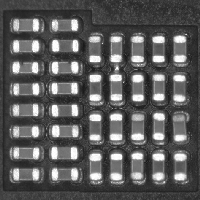
The solder paste material used was one that has been used in volume production—the only difference being that a Type 5 particle size was evaluated. This was a low-residue flux system with halogen-free, ROL0 (RO stands for rosin, L for low-activity, and zero for no detectible halides) materials. A Type 4 material was trialed, but the decision was made to use the Type 5 for this study. Figure 5 shows print comparisons.
Figure 5: Type 4 (L) and Type 5 (R) after printing.
Page 1 of 3
Share on:


Suggested Items
AIM Solder Appoints Mhanny Aguillo as Southeast Asia Technical Sales Manager
05/31/2024 | AIMAIM Solder, a leading global manufacturer of solder assembly materials, is pleased to announce the appointment of Mhanny Aguillo as the Southeast Asia Technical Sales Manager.
Merlin Flex Invests in New Techwin Solder Mask Developer
05/31/2024 | Merlin Flex LtdMerlin Flex Continue their investment programme with the installation & commissioning of a new Techwin Solder Mask Developer. This new machine allows faster & more accurate developing in the solder mask process.
IPC Hand Soldering Competition Thailand 2024
05/29/2024 | IPCIPC’s hand soldering competitions around the world are highly popular events generating a lot of attention, participation and publicity. The competition attracts the enthusiastic participation of thousands of professionals specializing in high-reliability products within the electronics industry such as defense, aerospace/aviation, rail transportation, automotive electronics, consumer electronics, etc.
AIM Solder Joins International Electronics Manufacturing Initiative (iNEMI)
05/29/2024 | AIMAIM Solder, a leading global manufacturer of solder assembly materials, is proud to announce its membership with the International Electronics Manufacturing Initiative (iNEMI).
Real Time with… IPC APEX EXPO 2024: Advanced Technologies with BlueRing Stencils
05/28/2024 | Real Time with...IPC APEX EXPOGuest Editor Kelly Dack and Greg Smith, manager of stencil technology with BlueRing Stencils, discuss the company's capabilities and services. They explore the use of nano coatings for thin stencils and determining the area ratio. Greg emphasizes the role of stencil artwork in controlling solder deposition and the need for collaboration between designers and stencil companies. They also focus on thinner stencils and step stenciling techniques for achieving proper solder deposition.