


 The Knowledge Base: A CM’s Perspective on Box Build Practices
 SMT Prospects and Perspectives: AI Opportunities, Challenges, and Possibilities, Part 1
 Nolan’s Notes: Do More, Get More
Approaches to Overcome Nodules and Scratches on Wire-Bondable Plating on PCBs
July 17, 2019 | Young K. Song and Vanja Bukva, Teledyne Dalsa Inc., and Ryan Wong, FTG CircuitsEstimated reading time: 4 minutes
Abstract
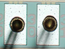
Initially adopted internal specifications for acceptance of printed circuit boards (PCBs) used for wire bonding was that there were no nodules or scratches allowed on the wirebond pads when inspected under 20X magnification. The nodules and scratches were not defined by measurable dimensions and were considered to be unacceptable if there was any sign of a visual blemish on wire-bondable features. Analysis of the yield at a PCB manufacturer monitored monthly for over two years indicated that the target yield could not be achieved, and the main reasons for yield loss were due to nodules and scratches on the wirebonding pads.
The PCB manufacturer attempted to eliminate nodules and scratches. First, a light-scrubbing step was added after electroless copper plating to remove any co-deposited fine particles that acted as a seed for nodules at the time of copper plating. Then, the electrolytic copper plating tank was emptied, fully cleaned, and filtered to eliminate the possibility of co-deposited particles in the electroplating process. Both actions greatly reduced the density of the nodules but did not fully eliminate them. Even though there was only one nodule on any wire-bonding pad, the board was still considered a reject. To reduce scratches on wirebonding pads, the PCB manufacturer utilized foam trays after routing the boards so that they did not make direct contact with other boards. This action significantly reduced the scratches on wire-bonding pads, even though some isolated scratches still appeared from time to time, which caused the boards to be rejected. Even with these significant improvements, the target yield remained unachievable.
Another approach was then taken to consider if wire bonding could be successfully performed over nodules and scratches and if there was a dimensional threshold where wire bonding could be successful. A gold ball bonding process called either stand-off-stitch bonding (SSB) or ball-stitch-on-ball bonding (BSOB) was used to determine the effects of nodules and scratches on wire bonds. The dimension of nodules, including height, and the size of scratches, including width, were measured before wire bonding. Wire bonding was then performed directly on various sizes of nodules and scratches on the bonding pad, and the evaluation of wire bonds was conducted using wire pull tests before and after reliability testing. Based on the results of the wire-bonding evaluation, the internal specification for nodules and scratches for wirebondable PCBs was modified to allow nodules and scratches with a certain height and a width limitation compared to initially adopted internal specifications of no nodules and no scratches. Such an approach resulted in improved yield at the PCB manufacturer.
Introduction
The development of the chip-on-board (COB) type of image sensors has significantly increased in the last few years to accommodate an increasing demand for low-cost, high-performance industrial inspection cameras. Wire bonding is the most commonly used technology for making the electrical interconnection between a silicon image sensor and its substrate during image sensor fabrication. Therefore, wire bonding directly on the PCB surface is inevitable for COB-type image sensor fabrication.
IPC-A-600J section 2.7.1.3—surface plating, wire-bond pads [1]—states, “Wire-bond pads are free of surface nodules, roughness, electrical test witness marks or scratches that exceed 0.8 mm (32 min) RMS (root-mean-square) in the pristine area in accordance with an applicable test method AABUS.” Since the tolerance of surface nodules (<0.8 mm RMS) in IPC-A-600J for wire bonding pads is not easily measurable and may not properly reflect single nodules and shallow scratches, the initially adopted specification for wire bonding pads as a user was defined to be free of surface nodules and scratches.
Figure 1: Average yield loss from multiple wire-bonding PCB products.
Therefore, a board was considered a reject if a nodule or a scratch was visible in the pristine area of the wire-bond at 20X magnification. If in any doubt, one could use 40X magnification for inspection to clarify pass/fail. However, in reality, it was difficult to achieve a wire-bonding surface in specification without nodules or scratches, resulting in low yield at the PCB manufacturer. In particular, PCB products designed with a center cut-out slot close to bonding pads were prone to significant yield loss due to nodules.
Yield review with the manufacturer and the analysis of causes for rejects using Pareto charts pointed out that two main reasons for PCB rejects were due to nodules and scratches on the wire-bonding surface. Yield had been reviewed on a monthly basis for 28 months, and the major yield losses continued to be due to nodules and scratches on the wire-bonding surface during the period. Figure 1 shows the average yield loss per month for wire-bonding boards due to nodules and scratches. The average yield losses from multiple PCB products due to nodules and scratches for wire bonding boards were in the range of 4–41% and 2–30%, respectively, during the period.
It is worth noting that the data in Figure 1 may not necessarily provide the picture of actual average yield loss due to nodules and scratches. When any defect—either nodule or scratch—was first found during an inspection of a board, the reason for rejection was recorded and further inspection of that board was not pursued since the board was already determined to be a reject. For example, the manufacturer recorded a 39% yield loss for nodules and none for scratches in Period 3. However, it may not mean that there were no scratches on those rejected boards since those boards had not been inspected further for scratches after nodules were first observed.
To read the full article, which appeared in the July 2019 issue of SMT007 Magazine, click here.
Share on:


Suggested Items
The Chemical Connection: Reducing Etch System Water Usage, Part 2
05/02/2024 | Don Ball -- Column: The Chemical ConnectionIn my last column, I reviewed some relatively simple ways to reduce water usage in existing etch systems: cutting down cooling coil water flow, adding chillers to replace plant water for cooling, lowering flow rate nozzles for rinses, etc. This month, I’ll continue with more ways to control water usage in your etcher. Most of these are not easily retrofittable to existing equipment but should be given serious consideration when new equipment is contemplated. With the right combination of add-ons, it is possible to bring the amount of water used in an etch system to almost zero.
Designer’s Notebook: What Designers Need to Know About Manufacturing, Part 2
04/24/2024 | Vern Solberg -- Column: Designer's NotebookThe printed circuit board (PCB) is the primary base element for providing the interconnect platform for mounting and electrically joining electronic components. When assessing PCB design complexity, first consider the component area and board area ratio. If the surface area for the component interface is restricted, it may justify adopting multilayer or multilayer sequential buildup (SBU) PCB fabrication to enable a more efficient sub-surface circuit interconnect.
Insulectro’s 'Storekeepers' Extend Their Welcome to Technology Village at IPC APEX EXPO
04/03/2024 | InsulectroInsulectro, the largest distributor of materials for use in the manufacture of PCBs and printed electronics, welcomes attendees to its TECHNOLOGY VILLAGE during this year’s IPC APEX EXPO at the Anaheim Convention Center, April 9-11, 2024.
ENNOVI Introduces a New Flexible Circuit Production Process for Low Voltage Connectivity in EV Battery Cell Contacting Systems
04/03/2024 | PRNewswireENNOVI, a mobility electrification solutions partner, introduces a more advanced and sustainable way of producing flexible circuits for low voltage signals in electric vehicle (EV) battery cell contacting systems.
Heavy Copper PCBs: Bridging the Gap Between Design and Fabrication, Part 1
04/01/2024 | Yash Sutariya, Saturn Electronics ServicesThey call me Sparky. This is due to my talent for getting shocked by a variety of voltages and because I cannot seem to keep my hands out of power control cabinets. While I do not have the time to throw the knife switch to the off position, that doesn’t stop me from sticking screwdrivers into the fuse boxes. In all honesty, I’m lucky to be alive. Fortunately, I also have a talent for building high-voltage heavy copper circuit boards. Since this is where I spend most of my time, I can guide you through some potential design for manufacturability (DFM) hazards you may encounter with heavy copper design.