


 Global Citizenship: Redefining Connection and Responsibility in Digital Transformation
 SMT Perspectives and Prospects: Artificial Intelligence, Part 5: Brain, Mind, Intelligence
 Global Sourcing Spotlight: Watch Out! Avoiding Pitfalls in Global Sourcing


Plasmatreat on Atmospheric Pressure Plasma
July 20, 2018 | Barry Matties, I-Connect007Estimated reading time: 4 minutes
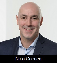
At the recent SMT Hybrid Packaging 2018 event held in Nuremberg, Germany, I sat down with Nico Coenen, global business development manager of Plasmatreat, for a discussion on Plasmatreat's atmospheric pressure plasma (AP plasma) treatment process and its various applications in the electronics industry.
Barry Matties: Nico, please tell us a bit about Plasmatreat.
Nico Coenen: Plasmatreat is a family-owned business, and we actually introduced atmospheric pressure plasma (AP plasma) in the industrial world. I think a lot of people are familiar with low pressure plasma. AP plasma has similar functionalities and can be used for cleaning, activation and deposition. It is easier to use because you can incorporate it in any kind of inline systems, robot handling, multiple systems, and so on.
Matties: It sounds really cost-efficient.
Coenen: It is very cost-efficient. There are very few consumable parts and the only thing you need is compressed air and electricity.
Matties: Why would someone choose vacuum and not atmospheric? What’s the advantage of vacuum?
Coenen: In the vacuum, you typically have a wider choice of different gases that you can use. You would also have a longer process in vacuum. If you have a tougher cleaning process that is needed, you might need to have a vacuum process. With low pressure plasma you have a large volume of homogeneous plasma whereas with atmospheric pressure plasma you achieve an intense area-selective treatment. A vacuum chamber is perfect for doing batch processes, whereas AP plasma jet systems are designed for continuous production.
Matties: Let's say I'm an assembler of circuit boards and I need to pretreat my boards. What would be an appropriate solution?
Coenen: We have multiple solutions. One is for PCB manufacturing where you have the typical cleaning for desmear or you want to activate your solder mask layer, and so on. These are for the printed circuit board manufacturers. For PCB assembly people, we see a lot of applications for pre-conformal coating. Typically, there are issues with the coating, whether it's bubbles, delamination, or cracking. You can prevent these kinds of typical issues seen on the conformal coating by first doing a surface activation with atmospheric plasma.
Matties: Right. Because it's inline, it's a quick process as well.
Coenen: It is a standard process that doesn't have any impact on your cycle time. We have run multiple tests where we compared the cycle time for a typical coating process versus a process with atmospheric plasma and they are similar.
Matties: What's the demands for AP plasma treatment these days? Are you seeing more inquiries about that?
Coenen: I do see a lot more inquiries on the coating side. This is for many reasons. Firstly, the conformal coating market is still increasing. Secondly, there is a change regarding the materials used. There is a trend toward thicker coatings. The thicker the coating is, the more difficult it is for it to adhere well. A thin coating with solvent base has very good adhesion. If you go for a thicker coating, those typically are not solvent-based and are more difficult to adhere to the surfaces. These are all elements in favor of doing an extra treatment step before the conformal coating.
Matties: Plasmatreat has been around for many years, right?
Coenen: Yes, for almost 25 years, the company was founded in 1995.
Matties: And you serve the global market, correct?
Coenen: Yes, the Plasmatreat Group, headquartered in Germany, has technology centers in Germany, the USA, Canada, China, Japan and Singapore as well as subsidiaries and sales partners in 35 countries. Just recently Plasmatreat set up a new subsidiary in South-Korea.
Matties: In terms of the inline treatment, is this a new concept for people to look at? Or is this something that they were already aware of, something that there's a demand for?
Coenen: Typically, the electronics market is very familiar with vacuum plasma because that's what they have been using in the semiconductor area. The atmospheric plasma isn't as popular within the electronics industry. That is actually my job: to highlight the capabilities and the potential that atmospheric plasma has within the electronics industry.
Matties: Because it's inline, what ramifications or impact are they going to have on installing it? Does it mean they have to reorganize their line to integrate this?
Coenen: No, and that’s the nice thing: You can integrate it into existing lines. If it's a standard PCB line, you just add a module within that line. We can integrate it in certain robots, like a coating robot that has a place for an extra tool, and so on. From an integration point of view, a lot of systems are being sold to automation companies that do integration for customers. It's very easy to integrate, and you can put it upside-down, bottom up, sideways, and with multiple jets. On the other hand our plasma systems can be installed off-line just as well. The opportunities are almost unlimited.
Matties: Is there anything else you would like to share with the industry?
Coenen: Yes. People usually think about plasma cleaning, but it's not just cleaning. There are a lot of applications where we can activate the surface. This activation can be making the surface hydrophobic or hydrophilic, depending on what kind of need you have. We also do functional nanocoating and there are several applications, such as anti-corrosion or for bonding metal to plastic. There are many coating applications that I think would suit the electronics industry well.
Matties: Great, a few value-adds there.
Coenen: I think so.
Matties: Nico, congratulations on your new position, and best of luck to you.
Coenen: Thank you.
Share on:


Suggested Items
KOKI Announces Upcoming Webinar on Solder Voiding – Causes and Remedies
04/16/2025 | KOKIKOKI, a global leader in advanced soldering materials and process optimization services, is pleased to announce its upcoming webinar, “Solder Voiding—Causes and Remedies,” which will take place on Tuesday, April 22, 2025, at 12:00 PM CDT. Jerome McIntyre, Regional Sales & Applications Engineer at KOKI Americas, will present this live session.
Real Time with... IPC APEX EXPO 2025: Transition Automation Focusing on Security Coatings and Squeegee Technology
04/16/2025 | Real Time with...IPC APEX EXPOMark Curtin, President of Transition Automation, gives an update on recent innovations at his company. He highlights a record sales month and their new focus on security coatings to fight counterfeiting. Mark explains the engineering behind their durable squeegees, the importance of maintenance, and the value of considering overall costs over just price.
Indium to Feature Materials Solutions Powering Sustainability at PCIM Europe
04/15/2025 | Indium CorporationIndium Corporation specializes in power device packaging, offering a portfolio of advanced material solutions encompassing the entire assembly, including die-attach, top-side die interconnect, substrate-attach, package-attach, and PCB assembly.
BEST Inc to Host Soldering 101 Workshop at Illinois & Michigan Locations
04/15/2025 | BEST Inc.BEST Inc., a leader in electronic component services, training, and products is pleased to announce it will host multiple Soldering 101 workshops in its Rolling Meadows, Illinois and Lansing, Michigan locations.
Real Time with... IPC APEX EXPO 2025: Advancements in Inkjet Technology With Electra Polymers
04/14/2025 | Real Time with...IPC APEX EXPODon Monn from Electra Polymers discusses the evolution of inkjet technology since 2016, focusing on market changes and the reliability of inkjet products. He explains the additive inkjet process, which reduces waste and boosts efficiency. The conversation highlights Electra Polymers' strong market presence in North America and the importance of customer trust.