


 SMT Prospects and Perspectives: AI Opportunities, Challenges, and Possibilities, Part 1
 Nolan’s Notes: Do More, Get More
 Global Sourcing Spotlight: Don’t Be Afraid of Global Sourcing
Solder Paste Stencil Design for Optimal QFN Yield and Reliability
April 29, 2015 | Ben Gumpert, Lockheed MartinEstimated reading time: 13 minutes
Abstract
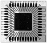
The use of bottom terminated components (BTC) has become widespread, specifically the use of Quad Flat No-lead (QFN) packages. The small outline and low height of this package type, improved electrical and thermal performance relative to older packaging technology, and low cost make the QFN/BTC attractive for many applications.
Over the past 15 years, the implementation of the QFN/BTC package has garnered a great amount of attention due to the assembly and inspection process challenges associated with the package. The difference in solder application parameters between the center pad and the perimeter pads complicates stencil design, and must be given special attention to balance the dissimilar requirements.
The lack of leads on the QFN/BTC package and the low standoff height result in significantly less compliance relative to other package types, making the QFN/BTC package more susceptible to CTE mismatch issues. Careful assembly of QFNs and proper printed circuit board (PCB) design can result in acceptable reliability depending on the overall design. One area that has not been well addressed, however, is the impact of die to package size ratio, and how this factor should be considered in circuit card assembly. IPC-7093 mentions the inverse relationship between relative die size and reliability, and Syed and Kang found the relationship to be non-linear, yet die size is seldom noted in component datasheets, and vendor recommendations do not include this ratio as a factor in assembly.
In this study, the volume of solder used in assembly of two QFN/BTC packages will be varied to investigate the relationship between standoff height and thermal cycle life, and to determine acceptable process limits with respect to first-pass yields. The QFNs selected have dissimilar die to package size ratios to assess the impact of this factor on the process window. Solder joint defect levels and thermal cycle results will indicate the ability to adjust manufacturing parameters to achieve a balance between the two objectives of process yield and reliability. The results will define a process window that provides the optimal installation of these packages.
Introduction
A wealth of information is available for optimizing PCB design and assembly for QFN packages, and this industry knowledge has been well cataloged in IPC-7093 [1]. This guideline reflects the recommendations found in many of the major component vendor application notes [2-8]. These documents all agree with respect to the typical target conditions for the solder joint; a standoff height of 2-3 mils, which is generally achieved by printing 1:1 on the perimeter lands and with a 20%-50% reduction of solder paste coverage on the center pad (although some vendors give more specific recommendations within this range of solder reduction on the center pad). These parameters will generally provide a high first-pass yield while providing for a relatively robust joint. The trade-offs for adjusting solder paste are also often mentioned; decreasing the volume of solder paste can reduce solder defects such as bridging but can negatively impact reliability, while increasing solder volume can do the opposite. Significant increases to the solder volume, however, can cause the component to float, potentially creating opens or misalignment.
One QFN/BTC property that is briefly mentioned in IPC-7093 and which been demonstrated to have a significant impact on QFN reliability is die size, or die to package ratio [9-11]. Component datasheets do not typically include information on the size of the die, but a sample of QFNs from several component vendors exhibited die to body ratios ranging from 0.27 to 0.58.
For the circuit card assembler, most of the decisions related to ensuring the best potential reliability of the QFN package have already been determined through design of the component package itself and of the PCB footprint. Once the design makes it to the point of assembly, the assembler has limited options to impact reliability, and these are dominated by stencil design (to affect standoff height and solder joint configuration). Standoff height can be controlled in several ways (bumping, use of preforms, stencil modification). Although standoff height is one of the standard recommendations from IPC-7093 and component vendors (2-3 mil), fillet formation is also recommended [10-13]. Kim et al. [12] concluded that a large fillet was preferred when increasing stand-off height of the component which was achieved at the expense of the fillet size.
Given the number of characteristics related to QFNs and their implementation that can impact reliability, it is unclear whether an assembler can apply a standard set of rules for installing QFNs onto a PCB, or if they must be evaluated on a case by case basis. Should the assembler adjust stencil apertures based on other design criteria, or should the standard 20-50% reduction of solder on the center pad be followed regardless, and if so, what value in that range is most desirable? Or should a greater reduction of solder paste be applied such that stand-off height is sacrificed to ensure large, convex fillets?
In this study, two QFN/BTC packages were evaluated for robustness of solder joints relative to changes to solder joint height controlled by center pad solder paste reduction. Extreme levels of solder variation (outside of the typical 20-50% reduction) were employed to demonstrate the amount of influence this factor may have and the points at which assembly defects may become important.
Experimental Procedure
The PWB selected for this study is a commercially available QFN/BTC style package test board. The board is constructed of FR-4 epoxy laminate, is two-sided (although only one side will be used in this study), is 0.062 inch thick, and has a HASL finish over copper. Approximate X-Y CTE is 11-13 ppm/°C. Two QFN style component packages will be used. These components have daisy chain circuitry to match the PWB, and have the parameters shown in Table 1.
Page 1 of 4
Share on:


Suggested Items
Vicor Power Orders Hentec Industries/RPS Automation Pulsar Solderability Testing System
04/24/2024 | Hentec Industries/RPS AutomationHentec Industries/RPS Automation, a leading manufacturer of selective soldering, lead tinning and solderability test equipment, is pleased to announce that Vicor Power has finalized the purchase of a Pulsar solderability testing system.
AIM Solder’s Dillon Zhu to Present on Ultraminiature Soldering at SMTA China East
04/22/2024 | AIMAIM Solder, a leading global manufacturer of solder assembly materials for the electronics industry, is pleased to announce that Dillon Zhu will present on the topic: Ultraminiature Soldering: Techniques, Technologies, and Standards at SMTA China East. This event is being held at the Shanghai World Expo Exhibition & Convention Center from April 24-25.
AIM to Highlight NC259FPA Ultrafine No Clean Solder Paste at SMTA Wisconsin Expo & Tech Forum
04/18/2024 | AIMAIM Solder, a leading global manufacturer of solder assembly materials for the electronics industry, is pleased to announce its participation in the upcoming SMTA Wisconsin Expo & Tech Forum taking place on May 7 at the Four Points by Sheraton | Milwaukee Airport, in Milwaukee, Wisconsin.
Hentec/RPS Publishes an Essential Guide to Selective Soldering Processing Tech Paper
04/17/2024 | Hentec Industries/RPS AutomationHentec Industries/RPS Automation, a leading manufacturer of selective soldering, lead tinning and solderability test equipment, announces that it has published a technical paper describing the critical process parameters that need to be optimized to ensure optimal results and guarantee the utmost in end-product quality.
Empowering Electronics Assembly: Introducing ALPHA Innolot MXE Alloy
04/16/2024 | MacDermid Alpha Electronics SolutionsIn the rapidly evolving electronics industry, where innovation drives progress, MacDermid Alpha Electronics Solutions is committed to setting a new standard. Today, we are pleased to introduce ALPHA Innolot MXE, a revolutionary alloy meticulously engineered to address the critical needs of enhanced reliability and performance in modern electronic assemblies.