


 SMT Prospects and Perspectives: AI Opportunities, Challenges, and Possibilities, Part 1
 Nolan’s Notes: Do More, Get More
 Global Sourcing Spotlight: Don’t Be Afraid of Global Sourcing
A Review of the Opportunities and Processes for Printed Electronics (Part 3): Materials, Process Developments
June 24, 2015 | Happy Holden, PCB Technologist-RetiredEstimated reading time: 10 minutes

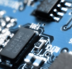
Most of the attention given to materials has appropriately centered on conductive inks, especially silver. Silver is the most conductive commonly used metal for making circuit conductors. Membrane switch circuits, which operate at relatively high voltages and low currents, have been printed onto polyester base materials using silver inks for more than a few decades. The challenge has been getting these circuits to have the bulk conductivity associated with copper. Common inks have conductivities that hover around 10% of copper and are not generally suitable for higher performance applications that operate at lower voltages or may require more power.
A number of suppliers have attacked the problem using a combination of new formulations of binders in the ink and nanoparticle silver are showing good improvements. One company, NovaCentrix, is addressing the challenge of making printable circuits by developing a tool and technology that sinters metal and semiconductor inks in a matter of milliseconds using light energy. The process reportedly can be carried out on a range of materials, including low-temperature, flexible substrates such as polyethylene terephthalate (PET) and paper. It is a promising technology for making low-cost products.
Ink technology
Organic and inorganic materials are both used for printed electronics. Ink materials must be available in liquid form for solution, dispersion or suspension. They must function as conductors, semiconductors, dielectrics or insulators. Material costs must be appropriate for the application.
For printing, viscosity, surface tension and solid content must be tightly controlled. Cross-layer interactions, such as wetting, adhesion, solubility and post-deposition drying procedures, affect the outcome. Additives often used in conventional printing inks are unavailable because they often defeat the purpose of electronic functionality.
Material properties largely determine the differences between printed and conventional electronics. Printable materials provide decisive advantages beside printability, such as mechanical flexibility and functional adjustment by chemical modification (e.g., light color in OLEDs).
Printed conductors offer lower conductivity and charge carrier mobility. With a few exceptions, inorganic ink materials are dispersions of metallic microparticles and nanoparticles. P-type metal-oxide-semiconductor (PMOS) technology may be used in printed electronics, but not complementary metal–oxide–semiconductor (CMOS) technology.
Conductive inks have been available for at least 40 years. The new conductive inks are designed specifically for use with low-temperature substrates including paper, (PET), polyether ether ketone (PEEK) and other plastics (including polyethylene film) and cure in an air environment.
Table 1: Ink Technologies
Copper, tin and silver nanoparticles are used with screen, flexo, offset and inkjet printing. Gold, silver and copper particles are used with inkjet. Sheet resistance is as low as ten milliohms per square. Resistivity’s as low as four times bulk have been attained with silver, but are higher for copper inks.
AC electroluminescent (EL) multicolor displays can cover many tens of square meters, or be incorporated into small watch faces and instrument displays. They involve six to eight printed inorganic layers, including a copper-doped phosphor, on a plastic film substrate.
Nanotechnology is the greatest boon to PE inks. There are proprietary material comprised of silicon nanoparticles dispersed in an environmentally-friendly blend of chemicals. These have optimized silicon particle size and dopant concentration to maximize the conversion efficiency of photovoltaic (PV) cells. The ink is screen-printed and a lower viscosity is available for inkjet printing.
Carbon nanotube (CNT) is another nanotechnology. CNT inks are available from many suppliers and known as V2V Ink Technology. C3Nano has transparent conductive CNT ink for touch panels and solar cells.
Table 2: Nanoparticle Conductive Metal Inks (from Novacentrix)
Substrates
Printed electronics uses flexible substrates, which lowers production cost and allows fabrication of mechanically flexible circuits. While inkjet and screen printing typically imprint rigid substrates like glass and silicon, mass printing methods nearly exclusively use flexible foil and paper. PET is a common choice due to its low cost and higher temperature stability. Polyethylene naphthalate (PEN) is another.
PEEK is a colorless organic polymer thermoplastic used in engineering applications. Polyimide (PI) foil is another alternative. Paper's low cost and manifold applications make it an attractive substrate, but its roughness and absorbency make it problematic for electronics. Low roughness and suitable wettability, which can be tuned pre-treatment (coating, corona) are important criteria for substrates. In contrast to conventional printing, high absorbency is usually disadvantageous.
Page 1 of 3
Share on:


Suggested Items
Janene Stinson, Boeing, Earns IPC Excellence in Education Award at IPC APEX EXPO 2024
04/22/2024 | IPCThe IPC Excellence in Education award was presented to Janene Stinson, Boeing, at IPC APEX EXPO 2024 in Anaheim, California, in recognition of her significant contributions to workforce development and leadership.
Zentech’s Board of Directors Announces the Return of Matt Turpin as President and CEO
04/22/2024 | Zentech ManufacturingTurpin draws upon over 35 years of experience in the electronics industry and has an 18-year history with Zentech. He previously served as President and CEO from 2006 to 2019 after which time he has remained active in the EMS industry as an advisor to Zentech and other industry organizations.
IDTechEx Report Unveils 3D Electronics Status and Opportunities
04/22/2024 | PRNewswire3D electronics is an emerging manufacturing approach that enables electronics to be integrated within or onto the surface of objects. 3D electronic manufacturing techniques empower new features, including mass customizability, greater integration, and improved sustainability in the electronics industry.
IDTechEx Examines the Opportunities for Wearables in Digital Health
04/19/2024 | IDTechExIDTechEx’s report, “Digital Health and Artificial Intelligence 2024-2034: Trends, Opportunities, and Outlook”, covers this ongoing trend in the consumer health wearables market and includes analysis of the opportunities and roadmap for biometric monitoring.
ZESTRON Welcomes Whitlock Associates as New Addition to their Existing Rep Team in Florida
04/19/2024 | ZESTRONZESTRON, the leading global provider of high-precision cleaning products, services, and training solutions in the electronics manufacturing and semiconductor industries, is thrilled to announce the addition of Whitlock Associates to its esteemed network of sales representatives.