


 SMT Prospects and Perspectives: AI Opportunities, Challenges, and Possibilities, Part 1
 Nolan’s Notes: Do More, Get More
 Global Sourcing Spotlight: Don’t Be Afraid of Global Sourcing
Averatek to Present 'Surface Treatment for Soldering Aluminum PCBs to Conventional Copper PCBs' at IPC APEX EXPO
October 29, 2021 | AveratekEstimated reading time: 1 minute
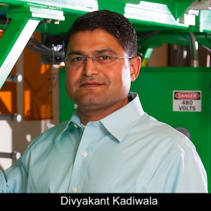
Averatek is pleased to announce that VP of Manufacturing Divyakant Kadiwala will present the paper entitled, “Surface Treatment for Soldering Aluminum PCBs to Conventional Copper PCBs” during the IPC APEX EXPO Technical Conference, scheduled to take place Jan. 22-27, 2022 at the San Diego Convention Center in California. The paper was co-authored by Nazarali Merchant, Ph.D., Senior Materials Scientist for Averatek.
Soldering is the preferred method for mounting SMDs and connecting circuit boards. But that brings in processing challenges. Soldering to aluminum requires an additional surface treatment or the use of conductive epoxy. These are cost-prohibitive and have reliability challenges and existing products like solders, fluxes, tack agents, cleaners etc. are formulated for Cu-PCBs and do not work on aluminum.
An advanced surface treatment technology will be presented that addresses all these constraints. Once printed on aluminum using conventional printing techniques such as screen, stencil etc., it is cured thermally in a convection oven at low temperatures, leaving a non-conductive deposit on the pads. This is followed by conventional process i.e. print solder over the treated pads, place components and then reflow resulting in finished Al-PCBs. It can also be used to solder Al-PCBs to flexible and rigid Cu-PCBs.
This is a paradigm shift in the industry which opens up many new applications, including those in the RFID, LED, and automotive industries. We will show solder cross-sections and shear data on the soldered joints, including Al-PET to Cu-PCB, Al-PET to Cu-Polyimide using aluminum metallization with low temperature Bi-Sn-Ag solders.
Kadiwala is a process development and project management leader in developing innovative products from laboratory concepts to large-scale manufacturing. He has 15+ years of multi-national experience with utilizing emerging technologies in strategic roles.
Kadiwala holds a BS in Chemical Engineering from the University of Mumbai, and a Master’s degree in Manufacturing Systems Engineering from the University of Wisconsin.
Merchant has 20 years of successful deliverables in PCBs, semiconductor packaging, metallurgy, welding consumables and processes, superconductors, fuel cells, batteries, solar cells, and failure analysis. His work has resulted in six US patents, three US patent applications under review, and 25 technical publications.
Merchant holds Doctorate and Master’s degree in Materials Engineering from the University of Illinois, and a Bachelor of Technology in Metallurgical Engineering from IIT of Bombay.
Share on:


Suggested Items
TTM Celebrates the Grand Opening of Its First Manufacturing Facility in Penang
04/25/2024 | TTM Technologies, Inc.TTM Technologies, Inc., a leading global manufacturer of technology solutions including mission systems, radio frequency (RF) components and RF microwave/microelectronic assemblies, and quick-turn and technologically advanced printed circuit boards (PCBs), officially opened its first manufacturing plant in Penang, Malaysia with an investment of USD200 million (approximately RM958 million).
Designer’s Notebook: What Designers Need to Know About Manufacturing, Part 2
04/24/2024 | Vern Solberg -- Column: Designer's NotebookThe printed circuit board (PCB) is the primary base element for providing the interconnect platform for mounting and electrically joining electronic components. When assessing PCB design complexity, first consider the component area and board area ratio. If the surface area for the component interface is restricted, it may justify adopting multilayer or multilayer sequential buildup (SBU) PCB fabrication to enable a more efficient sub-surface circuit interconnect.
Elevating PCB Design Engineering With IPC Programs
04/24/2024 | Cory Blaylock, IPCIn a monumental stride for the electronics manufacturing industry, IPC has successfully championed the recognition of the PCB Design Engineer as an official occupation by the U.S. Department of Labor (DOL). This pivotal achievement not only underscores the critical role of PCB design engineers within the technology landscape, but also marks the beginning of a transformative journey toward nurturing a robust, skilled workforce ready to propel our industry into the future.
IPC Design Competition Champion Crowned at IPC APEX EXPO 2024
04/24/2024 | IPCAt IPC APEX EXPO 2024 in Anaheim, California, five competitors squared off to determine who was the best of the best at PCB design.
Real Time with... IPC APEX EXPO 2024: all4-PCB, A Premier Solution Provider for the PCB Industry
04/22/2024 | Real Time with...IPC APEX EXPOIn the PCB industry, all4-PCB, is a top-tier equipment supplier and process solution provider. Ralph Jacobo highlights the active market and the demand for high-quality equipment, discusses their existing customers, investment in advanced substrates, and smaller board shops.