-

- News
- Books
Featured Books
- smt007 Magazine
Latest Issues
Current Issue
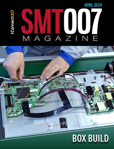
Box Build
One trend is to add box build and final assembly to your product offering. In this issue, we explore the opportunities and risks of adding system assembly to your service portfolio.

IPC APEX EXPO 2024 Pre-show
This month’s issue devotes its pages to a comprehensive preview of the IPC APEX EXPO 2024 event. Whether your role is technical or business, if you're new-to-the-industry or seasoned veteran, you'll find value throughout this program.

Boost Your Sales
Every part of your business can be evaluated as a process, including your sales funnel. Optimizing your selling process requires a coordinated effort between marketing and sales. In this issue, industry experts in marketing and sales offer their best advice on how to boost your sales efforts.
- Articles
- Columns
Search Console
- Links
- Events
||| MENU - smt007 Magazine
The Impact of Vias on PCB Assembly
November 17, 2016 | Stephen Las Marias, I-Connect007Estimated reading time: 1 minute
The continuing trend towards smaller and smaller devices with even more functionality has resulted in a dramatic reduction in the size of components, silicon packages, and the PCBs themselves. Component technologies such as BGAs and CSPs have challenged PCB manufacturing technologies due to the number of input/output connections and tighter and tighter pitches associated with these devices. Don’t forget the costs associated with fabrication.
Via technology—including blind and buried—has been one of the solutions to address the miniaturization and component density challenges in current electronic assemblies. Advantages include improved electrical and thermal performance; increased wiring density; space-saving in PCBs; placement of even more chips and components in PCBs; and finally, smaller PCBs.
Source: I-Connect007 Survey
However, vias are not without their own set of challenges. In our recent survey that focused on vias, respondents mentioned challenges such as impedance matching, routing, placement of vias, minimum size limitations, aspect ratio, and the limitations for the PCB manufacturer. One respondent commented: “In-pad vias in thermal pads and regular lands often cause processing issues. If they are tented, trapped residues and ‘popping’ are issues. If they are not tented, solder thieving is an issue. We have also tried using solder mask dams on the pad to prevent thieving with poor results. We also don't want to add more vias than necessary to meet the thermal target. In this case, more is not necessarily better as it may increase voiding at the thermal interface.” He added that more vias increase the drill time at the PCB fabricator side, and may increase cost.
Reliability is also an issue, per our survey. One respondent said that their QA department is concerned that tenting vias leaves contaminants in vias, which can affect the long-term reliability of the PCB assembly. He noted, though, that tenting vias help minimize solder problems, so he always tents vias. Apart from tenting, via filling, mask covering and plating are also challenges when dealing with vias.
To read this entire article, which appeared in the November 2016 issue of SMT Magazine, click here.
Suggested Items
Taiyo Circuit Automation Installs New DP3500 into Fuba Printed Circuits, Tunisia
04/25/2024 | Taiyo Circuit AutomationTaiyo Circuit Automation is proud to be partnered with Fuba Printed Circuits, Tunisia part of the OneTech Group of companies, a leading printed circuit board manufacturer based out of Bizerte, Tunisia, on their first installation of Taiyo Circuit Automation DP3500 coater.
Vicor Power Orders Hentec Industries/RPS Automation Pulsar Solderability Testing System
04/24/2024 | Hentec Industries/RPS AutomationHentec Industries/RPS Automation, a leading manufacturer of selective soldering, lead tinning and solderability test equipment, is pleased to announce that Vicor Power has finalized the purchase of a Pulsar solderability testing system.
AIM Solder’s Dillon Zhu to Present on Ultraminiature Soldering at SMTA China East
04/22/2024 | AIMAIM Solder, a leading global manufacturer of solder assembly materials for the electronics industry, is pleased to announce that Dillon Zhu will present on the topic: Ultraminiature Soldering: Techniques, Technologies, and Standards at SMTA China East. This event is being held at the Shanghai World Expo Exhibition & Convention Center from April 24-25.
AIM to Highlight NC259FPA Ultrafine No Clean Solder Paste at SMTA Wisconsin Expo & Tech Forum
04/18/2024 | AIMAIM Solder, a leading global manufacturer of solder assembly materials for the electronics industry, is pleased to announce its participation in the upcoming SMTA Wisconsin Expo & Tech Forum taking place on May 7 at the Four Points by Sheraton | Milwaukee Airport, in Milwaukee, Wisconsin.
Hentec/RPS Publishes an Essential Guide to Selective Soldering Processing Tech Paper
04/17/2024 | Hentec Industries/RPS AutomationHentec Industries/RPS Automation, a leading manufacturer of selective soldering, lead tinning and solderability test equipment, announces that it has published a technical paper describing the critical process parameters that need to be optimized to ensure optimal results and guarantee the utmost in end-product quality.


