


 SMT Prospects and Perspectives: AI Opportunities, Challenges, and Possibilities, Part 1
 Nolan’s Notes: Do More, Get More
 Global Sourcing Spotlight: Don’t Be Afraid of Global Sourcing
Dispensing EMI Shielding Materials: An Alternative to Sputtering
August 23, 2019 | Garrett Wong, Nordson Asymtek and Jinu Choi, Henkel Electronic Materials LlcEstimated reading time: 5 minutes
Abstract
Shielding electronic systems against electromagnetic interference (EMI) has become a hot topic. Technological advancements toward 5G standards, wireless charging of mobile electronics, in-package antenna integration, and system-in-package (SiP) adoption are driving the need to apply more effective EMI shielding and isolation to component packages and larger modules. For conformal shielding, EMI shielding materials for exterior package surfaces have mostly been applied with a physical vapor deposition (PVD) process of sputtering, leveraging front-end packaging technologies to back-end packaging applications. However, sputtering technology challenges in scalability and cost along with advancements in dispensable materials are driving considerations for alternative dispensing techniques for EMI shielding.
The authors will discuss the development of a spray coating process to apply EMI shielding materials to the exterior surfaces of individual components on strips and larger SiP packages. Using newly developed and enhanced materials and equipment for this industry, a process was demonstrated that provided uniform coating on packages in the sub-10-μm thickness range with consistent coating thicknesses around package corners and package sidewalls, producing a top surface-to-sidewall thickness ratio of 1:1. Further investigation showed decreased production costs for applying EMI shielding to component packages by increasing spray-coating productivity and by selectively applying the coating to specific areas of packages. Additionally, low capital-equipment expense and shorter lead times for spray coating equipment improved the ability to scale up production capacity compared to sputtering equipment.
In mobile electronics packaging, several SiP-module manufacturers are challenged to isolate components within the SiP from each other and from their exterior for EMI shielding. Trenches are cut around the interior components and conductive paste is dispensed into the trenches to form smaller Faraday cages within the package. As trench designs become narrower, it’s imperative to control both the volume and placement accuracy of the material filling the trenches. The latest, advanced jetting products provide control of the volume while the narrow, in-air stream width delivers accurate trench fill. In a final step, the tops of these paste-filled trenches are connected by applying exterior EMI shield coating. Spraying overcomes challenges faced when using sputtering equipment and harnesses the improvements in both the EMI shielding materials and the equipment for depositing it so that SiP packages can be manufactured using efficient back-end packaging techniques.
Introduction: Growth of EMI Shielding
EMI shielding has become a topic of significant interest in recent years. As 5G wireless technology is approaching mass-market acceptance and the future capabilities 5G standards will enable for the internet of things (IoT) and mission-critical communications, there is a significantly increasing need to effectively shield electronics and components from EMI. With the upcoming 5G wireless standards, signal frequencies of 600 MHz to 6 GHz and mmWave bands will become increasingly more common and powerful as the technology is adopted. Some of the proposed uses and implementations include window panels for office buildings or public transportation to help deal with shorter range communications.
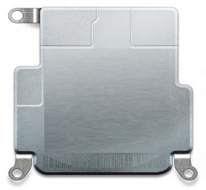
Figure 1: Example SiP unit with sputter coating and integrated EMI shielding structures.
Other proposed implementations include home and office building repeaters to provide adequate coverage due to 5G frequencies having difficulties passing through walls and other solid objects. All of this activity will lead to an increased prevalence of signals in the 5G frequency range and a higher risk of exposure to EMI in these frequency ranges and their harmonics.
Fortunately, EMI can be shielded on component and system-in-package (SiP) devices through the application of thin coatings of conductive metal to the exteriors of such devices (Figure 1). Historically, EMI shielding has been applied through placing stamped metal cans around groups of components or by applying EMI shielding tapes to specific components. However, as packages and end devices continue to become miniaturized, such shielding methods become prohibitive due to size constraints as well as the flexibility to handle diverse, non-orthogonal packaging concepts that are becoming more common in mobile and wearable electronics.
Likewise, some leading-edge package designs are moving toward selective coating of only certain areas of a package for the EMI shielding rather than a complete shell over the full exterior of the package. In addition to the external coating for the EMI shielding, new SiP devices are further requiring additional integrated shielding to be built directly into the package to properly isolate individual components from each other in a single package.
Sputtering: A Method of Applying EMI Shielding
The predominant method for creating EMI shielding on molded component packages or molded SiP devices has been through sputtering multiple layers of metals over the surface. With sputtering, it has been possible to apply very thin, consistent coatings of pure metal or metal alloys to package surfaces in the 1-7μm thickness range. With the nature of the sputtering process capable of depositing metals at the angstrom level, the electrical performance of its coating layer has been effective thus far for typical shielding application.
However, as the need for shielding grows, sputtering has significant inherent drawbacks for it to be established as a scalable method for manufacturers and designers. Initial capital equipment costs for sputtering equipment are very high-in the million-dollar range. Sputter equipment lines require significant floor space due to its multi-chamber process, and further increases the need for additional real estate with full in-line conveyorized systems. With the inciting of plasma to sputter material from a sputter target to the substrate, typical sputter chamber environments could reach into the 400°C range; therefore, cooling of a substrate with a “cold plate” mounting fixture to reduce the experienced temperatures is needed. The sputtering process deposits metal on a given substrate but typically only produces up to 60% thickness coverage on the vertical sidewalls of a three-dimensional package compared to the thickness of the top surface layer.
Lastly, due to the nature of sputtering being a line-of-sight deposition process, metal particles cannot be selectively applied or necessarily applied under overhanging structures and topology and can result in significant material wastage in addition to material accumulation inside of the chamber walls; hence, this requires intensive maintenance. It is also necessary to pre-apply masking to substrates if there are specific areas of a given substrate that must remain exposed or do not require EMI shielding.
To read the full article, which appeared in the August 2019 issue of SMT007 Magazine, click here.
Share on:


Suggested Items
Real Time with... IPC APEX EXPO 2024: all4-PCB, A Premier Solution Provider for the PCB Industry
04/22/2024 | Real Time with...IPC APEX EXPOIn the PCB industry, all4-PCB, is a top-tier equipment supplier and process solution provider. Ralph Jacobo highlights the active market and the demand for high-quality equipment, discusses their existing customers, investment in advanced substrates, and smaller board shops.
Global Semiconductor Equipment Billings Slip to $106.3 Billion in 2023
04/10/2024 | SEMIWorldwide sales of semiconductor manufacturing equipment edged down 1.3% to $106.3 billion in 2023 from an all-time record of $107.6 billion in 2022, SEMI, the industry association representing the global electronics design and manufacturing supply chain, reported today. The data is now available in the Worldwide Semiconductor Equipment Market Statistics (WWSEMS) report.
iNEMI Unified Equipment Interaction Methodology Webinar
04/10/2024 | iNEMIiNEMI’s Unified Equipment Interaction Methodology Project was a collaboration between manufacturers and equipment suppliers to validate the feasibility and ease of implementation of SEMI standards being developed as part of the SEMI North America Fab & Equipment Computer and Device Security Task Force (CDS).
SCHMID Group Presents Breakthrough Solutions for Substrate Production at ISES USA
04/09/2024 | SCHMID GroupThe SCHMID Group, a global leader in providing solutions to the high-tech electronics, photovoltaics, glass, and energy systems industries participated in the International Semiconductor Executive Summit (ISES) USA this week.
Calumet Electronics Boosts PCB Production Capacity with Strategic CapX
04/05/2024 | Calumet ElectronicsCalumet Electronics is proud to announce a significant expansion of its domestic printed circuit board (PCB) production capacity at its campus in Michigan’s Upper Peninsula. Over the last four years, Calumet has strategically invested in manufacturing equipment, workforce development, and campus expansion.