-

- News
- Books
Featured Books
- smt007 Magazine
Latest Issues
Current Issue
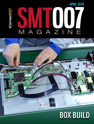
Box Build
One trend is to add box build and final assembly to your product offering. In this issue, we explore the opportunities and risks of adding system assembly to your service portfolio.

IPC APEX EXPO 2024 Pre-show
This month’s issue devotes its pages to a comprehensive preview of the IPC APEX EXPO 2024 event. Whether your role is technical or business, if you're new-to-the-industry or seasoned veteran, you'll find value throughout this program.

Boost Your Sales
Every part of your business can be evaluated as a process, including your sales funnel. Optimizing your selling process requires a coordinated effort between marketing and sales. In this issue, industry experts in marketing and sales offer their best advice on how to boost your sales efforts.
- Articles
- Columns
Search Console
- Links
- Events
||| MENU - smt007 Magazine
Copyright © 2024 I-Connect007 | IPC Publishing Group Inc. All rights reserved.
Log in


