


 Global Sourcing Spotlight: Golf, Friedman, and the Benefits of Global Sourcing
 Nolan’s Notes: Coming to Terms With AI
 The Knowledge Base: A CM’s Perspective on Box Build Practices
Diode Laser Soldering Technology: The Next Generation in Non-Contact Soldering
December 31, 1969 |Estimated reading time: 7 minutes
With development of newer reduced cost, high-power diode lasers, selective soldering with laser now is gaining wider acceptance for production of miniaturized interconnects.
By Gary Goldberg
Lead-free soldering is a response to proposed legislative restrictions on the use of lead in electronics in the Far East and Europe. This article compares tin-lead and lead-free soldering using the widely accepted original heat source, Xeon arc heating lamp (also known as Soft Beam) and the newer diode laser heat source.
Diode lasers are becoming an increasingly attractive option for selective soldering in microelectronics, due in part to their increased reliability, better electrical conversion efficiency and cost-effectiveness. The other optical soldering technology, Xeon arc Soft Beam heating lamp has been on the market for years. Both optical soldering technologies have their inherent advantages over traditional selective wave technologies because of their non-contact nature.
Most laser soldering systems currently used produce joints sequentially, as opposed to conventional soldering processes such as wave soldering. Sequential soldering of single joints normally requires less than 10 W, falling within the power range of diode laser devices.
Soft Beam is the type of light from a Xeon arc amp that is passed through an optical fiber 5 mm in diameter, which is connected to a converging lens, focusing the light beam to a spot diameter of 1 mm. The spectral content of the Xeon arc lamp is spread over a wavelength range between 350 to 1,100 nm, while the laser diode is highly monochromatic at 810 and 940 nm. Thus, the laser diode has a higher power density/convergence compared to short-arc heating lamps. A diode laser output could be focused to a much smaller spot diameter (~0.4 mm) than the light beam heater's light (1 mm).
Diode Laser Soldering
An important advantage of diode laser soldering is its ability to focus the energy beam specifically onto the workpiece with minimal heating of the surrounding parts. It has a small heat-affected zone, meaning less heating of the board. Thus, it is targeted for use when heat-sensitive components are near the part to be soldered. The technology avoids the need to preheat components when high thermal mass substances must be soldered. Further, rapid heating and cooling of the solder results in fine-grained solder micro-structure, with improved mechanical properties.
Lead-free Soldering
Lead-free soldering is being introduced on a wide-scale basis as a response to worldwide legislative restrictions on the use of lead in electronics. Various alternatives have been proposed, but the tin-silver (SnAg) group of alloys has been shown to be functionally equivalent to tin-lead (SnPb) ones in certain situations, although there is still some concern over replacements for higher-temperature (~300°C) lead-based solders. However, a combination of factors, such as availability, mechanical properties and melting point led to choosing tin-silver (96.5 percent Sn, 3.5 percent Ag) as the material composition to study.
To evaluate solder joint quality, predict cycle time and select process parameters, modeling the thermal dynamic response of the solder joint is critical. In an earlier research work, 1 a mathematical model was developed for a through-hole laser soldering process to determine the thermal signatures of the solder. The lumped-parameter model can be used to study the temperature response of the solder, as well as the component under different process parameters, such as laser power and pulse duration.
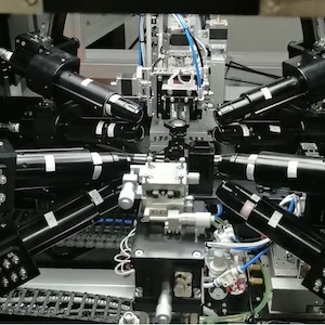
A direct-diode laser and Xeon arc-heating lamp were integrated into robots to develop automated selective soldering machines of equal motion control and movement. This article compares the two heating technologies for both tin-lead as well as lead-free solders, and examines the quality of the finished solder joints.
Experiments with Tin-Lead Solders
Soldering experiments were conducted using a diode laser and Xeon arc-heating lamp for 60-40 tin-lead solder. A 25 W diode laser was used to conduct the soldering experiments. The heart of the system is a diode laser system.*
A fiber array package (FAP) module generates the diode laser beam. This module is built into the diode laser system. The work was performed using this standard commercially available system. In this case, the FAP module uses a diode bar emitting at 980 nm wavelength. The FAP module is built around a single, 19-emitter diode laser bar, with each emitter coupled into individual small-diameter fibers. These 19 fibers then are brought together into a flexible fiber bundle 800 µm in diameter. The delivery fiber is coupled to a standard optical imaging accessory (OIA). This OIA consists simply of two lenses: collimating and focusing, which produce a 1:1 image of the fiber tip at a working distance of 33 mm from the focusing lens.
 Figure 1. Closeup photo of the soldered joints with laser power of 25 W and pulse durations. (L-R) 0.8 sec, 0.8 sec, 1.0 sec, 1.0 sec, 1.0 sec, 1.0 sec and 1.0 sec.
The laser was connected to the Z-axis of a Cartesian robotic system, which was integrated with a micro camera to make a vision-guided laser soldering workstation. At a focal distance of 33 mm, the laser is focused to a spot diameter of 0.8 mm on top of the FR4 printed circuit board (PCB).
Tests were conducted at different power levels and pulse durations using 60-40 solder preforms, as shown in Figure 1. The PCB measures 89 × 51 × 1.5 mm, and the copper track is 0.25 mm thick. The component to be soldered is a standard resistor network.
 Figure 2. Joints soldered by Xeon arc-heating lamp at 60 W at different pulse durations. The right joint soldered at 0.5-sec pulse duration shows incomplete melting.
A 60-40 solder preform was used in the process. Dimensions of the solder preform are OD 1.90 × ID 1.20 × thickness 1.50 mm.
Experiments with Soft Beam and 60-40 Solder Wire
Similar soldering tests were conducted using the Xeon arc-heating lamp as a heating source (Figure 2 and Tables 1 and 2). Further experiments were carried out using 60-40 solder wire for different joints. For soldering a particular joint using a 60-40 solder preform, process parameters are:
- Short-arc heating lamp: 60 W/1 sec
- Diode laser: 25 W/0.8 sec

These results indicate that less power and a shorter heating time are required when using a diode laser.
Experiments with Lead-free Solder
A single standard solder joint configuration was used to demonstrate a generic experimental approach to minimizing heat input. A small FR4 circuit board was designed specifically for investigation into diode laser soldering. In addition, for this work, standard tin-plated copper through-holes at a pitch of 0.1" were provided on the board so that a standard 44-pin chip carrier could be soldered into the board.

To achieve reproducible solder joints, 1.7-mm OD (0.07") solder preforms were used. These preforms were selected over solder paste or solder wire feeding, as use of the preforms provides more reproducible results, especially in a laboratory environment. In this case, 96.5/3.5 percent tin-silver solder preforms were used,
with a melting point of 221°C. ** These are coated with an RMA-type low-solid flux, making it a no-clean solder. The solder preforms used were 0.61 mm thick, 1.65 mm OD and 0.56 mm ID, pre-placed by hand onto the pins. To ensure a valid optimization trial, soldering time was fixed at 0.8 sec, so average power and solder composition were the primary variables studied. Average power was changed in increments of 2 W over the range at which solder joints were produced. At each setting, a total of 13 pins were soldered. Results for lead-free solder joints over the optimum range of 6 to 12 W average power can be seen in Figures 3, 4, 5 and 6.
 Figure 3. SnAg solder, 12 W, 0.8 sec. Result: overheated joint. Figure 4. SnAg solder, 10 W, 0.8 sec. Result: optimal joint. Figure 5. SnAg solder, 8 W, 0.8 sec. Result: underheated joint. Figure 6. SnPb solder, 8 W, 0.8 sec. Result: optimal joint.
null
Inference
For this particular joint configuration, for a soldering time of 0.8 sec, using this lead-free solder composition, an average power of 10 W produces the best quality solder joint. When compared with a standard 60-40 SnPb solder composition, an increase of 2 W in average power is required to produce an optimized joint. This power increase helps achieve the increased temperature required for soldering higher melting point lead-free solders.
Conclusion
The latest diode laser system successfully soldered both lead-free and lead-containing solder joints with higher quality in less time. Thin, intermetallic layers and small grain size were observed on the diode laser-soldered joints, suggesting that the mechanical properties of the joints would be acceptable. Diode laser produces low-heat input joints for the type of through-hole electronic components used in this experiment.
The diode laser performed more quickly than the short-arc heating lamp in soldering speed. The diode laser (at 810 nm) could penetrate the solder efficiently, reducing the time required to create a good solder joint. Diode laser soldering systems may be useful in high-mix production areas that require both tin-lead and lead-free soldering capabilities.
*QUATTRO FAP system.** Alpha Fry Technologies.
References
- Syed Naveed, Robert Woods, "Diode Laser Soldering — A Lumped-Parameter Mathematical Model and Comparison of Different Soldering Technologies," Proceedings of the Conference on High-power Diode Laser Technologies and Applications, Photonics West 2003, San Jose, CA, January 2003.Coherent Semiconductor Division data sheet, FAP System.PRO-MATION and Spectra Technologies, Euless, Texas (Gary Goldberg, George Wood and Victor Trotter).
Gary Goldberg, president and CEO, may be contacted at Pro-mation Inc., (262) 942-4177; Fax (262) 942-0101; E-mail: Gary_Goldberg@pro-mation-inc.com; Web site: http://www.Pro-mation-Inc.com.
Share on:


