


 Global Sourcing Spotlight: Golf, Friedman, and the Benefits of Global Sourcing
 Nolan’s Notes: Coming to Terms With AI
 The Knowledge Base: A CM’s Perspective on Box Build Practices
Working Inside China
December 31, 1969 |Estimated reading time: 2 minutes
WILLOW GROVE, Pa. — Kulicke & Soffa, a leading wire bonding equipment supplier, recently established a manufacturing facility in Suzhou, China. Oded Lendner, vice president of K&S operations worldwide, shared his views on this new move in a recent conversation with SMT editors.
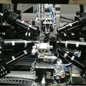
 Kulicke & Soffa's Suzhou facility.
"The motivation to establish a presence in China is twofold. One, we needed to establish a presence in a growing market region to become more competitive in the semiconductor industry; and two, from a manufacturing perspective, operations in China are more cost-effective for the company," says Lendner.
"Until 2000, most of our products were manufactured in the U.S.," he adds. "As the market became more competitive, we needed to improve costs and move closer to our Asian customer base. Initially, we moved manufacturing of our IC ball bonders to Singapore. However, after 2000, the market became even more challenging, with stronger pressure to reduce production costs.
"In July 2002, we opened a manufacturing facility in Suzhou, China, dedicated to the production of our more labor-intensive products," Lendner continues. "The first product we moved to our Suzhou plant was our capillary line, which was initially produced in Israel. Currently, our Suzhou facility manufactures approximately 60 percent of our worldwide capillary production. We recently began production of wafer test probe cards in our Suzhou facility and already have begun shipping probe cards to customers from China."
K&S is noted for wire bonders used in semiconductor assembly. The company also produces the wires and capillaries involved in the process as well as wafer test probes used to test components prior to assembly. The cantilever wafer test probes are labor-intensive, so production of these was moved to China. Ball bonders still are assembled in Singapore due to the skill sets and expertise of local workers, but approximately 40 percent of the major subcomponents are produced in China.
Going to Singapore in 2000 helped prepare K&S to establish new production facilities in China. The Suzhou Industrial Park itself is a joint venture between Singapore and China. Having a Mandarin-speaking management team assisted the eventual move to Suzhou. The infrastructure is still developing in China, but state-of-the-art industrial parks exist for companies like K&S. Many K&S customers such as AMD, Hitachi, Fairchild, National, Carsem, Intel, STATS ChipPAC and others are just starting operations or have already established manufacturing capability in this location.
In 2003, China represented 3 percent of the worldwide capacity for electronics packaging; by 2005, it will capture 9 percent. According to K&S, benefits associated with the cost of manufacturing in China are enormous and a catalyst for many semiconductor manufacturers moving into the country. While still in its early years of this new venture, K&S has already experienced great success in China. The Suzhou facility was able to ramp up production in July 2002 and ship 1 million capillaries by December 2003. "Today, we're already shipped about 2 million," says Lendner.
On the downside, the company must deal with high turnover. "All of our employees are local. We don't have dormitories," Lendner explains. "However, the turnover is high, at approximately 25 percent, because there's an unbelievable opportunity for those trained in electronics manufacturing. We tried stock options and offering long-term financial incentives. The Chinese employees are young, well educated, ambitious and need challenges. That can be both an asset and liability when dealing in the high-tech semiconductor market."
— Gail Flower
Share on:


