


 Global Sourcing Spotlight: Golf, Friedman, and the Benefits of Global Sourcing
 Nolan’s Notes: Coming to Terms With AI
 The Knowledge Base: A CM’s Perspective on Box Build Practices
Rework/Repair
December 31, 1969 |Estimated reading time: 17 minutes
By Matthew R. Milbury
With the continuing evolution toward smaller components, higher board densities and more diverse mixes, process equipment is stressed to the limits of its capabilities. In an industry where lead pitches and chip sizes are straining the naked eye, components are being mounted at ever-higher speeds. This means rework is a fact of life and will remain so well into the foreseeable future.
Repairing and reworking a substrate can be accomplished at any point during assembly. Inspection after stencil printing may find that pads have been skipped; inspection after placement may detect a bent or broken lead, or even a missing component. When the defect is noted, the board is typically removed from the line.
Though inspection also occurs after reflow soldering often at the end of the line, before testing finding defects at this point is difficult for the technician because the solder joints have been formed and the components are secured to the board. Today's rework stations have the capability to remove components with nozzles that direct heat at prescribed temperatures to the component interconnects. As a result, the solder "melts" without surrounding devices being affected. The component is then lifted from the board using a vacuum pickup incorporated in the nozzle. More sophisticated machines also incorporate vision alignment to ensure precision in mounting the replacement component.
Reworking components on boards is not restricted to leaded devices or even FR-4 substrates. Array components, such as ball grid arrays (BGA) and flip chips, can be removed and replaced. Flip chips can be reworked because testing of the components usually occurs prior to dispensing and curing of the underfill. For components where the underfill has been applied, the process is more complicated, as the epoxy is difficult to remove from the board.
Equipment Requirements for ReworkRework systems differ in design and capability. Certain features, however, are particularly important to successfully replace defective components in a production environment. As with assembly, the bottom line is cost and throughput, as well as passing inspection and test.
A fundamental requirement is for the process to be automated so the quality of the rework is independent of the skill and experience of the individual technician. Design features, such as programmable logic control and user-friendly software with a programmable head for picking and placing components, enable the desired level of automation. From an equipment standpoint, a flat platform for achieving coplanarity and an X-Y alignment system that ensures precision and repeatability in positioning are paramount. A rugged, machined structure is essential for stability and accurate alignment of the placement head, optics and table. Linear bearings are also preferred for precision movement of the X-Y table.
Substrate mounting should be in a holding fixture that permits the board to expand during heating, and the platform should incorporate adjustable supports for the underside of the board to prevent sagging because of heat and component weight. Other useful features include: thermal profiling, paste deposition, top and bottom heaters, nitrogen as well as air as the supplied process gas, and vision alignment. An efficient, large-area preheater is essential to prevent board warp, which commonly occurs when larger boards are subjected to localized heating.
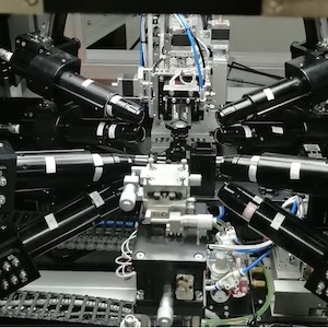
 Figure 1. This rework station enables removal and replacement of both leaded and area-array components, including BGAs and flip chips.
Removing Defective ComponentsThe rework machine in Figure 1 is a semiautomated floor model with Windows-based software, top- and bottom-forced convection heating with an integrated vacuum pickup in the nozzle, bottomside hot-gas process heater, large-area infrared (IR) preheater, and "component-to-pad" vision alignment. Air or nitrogen can be supplied as the process gas, depending on the rework requirement.To remove a defective component, the substrate is mounted in a holding fixture on the X-Y table and secured in position with thumb screws. Spring-loaded clamps in the fixture permit the board to expand during heating. When working on a double-sided board, bottom board supports are adjusted to avoid components on the underside and raised to the height required to prevent the substrate from sagging.The removal of a component is assisted by a series of "prompts" shown on the computer screen. Each component type and size requires a different profile; the parameters for the profile are stored in memory. Parameters for heating include: temperature and velocity of the gas for the top and bottom heaters; distance of the top heater above the board; use of the bottomside IR preheater; and the time (how long the heater is at its "setpoint"). After logging on, the operator selects the nozzle specified during the prompts, installs it in the heater head, aligns the nozzle over the component and runs the correct profile. While a series of "templates" (sample profiles) may be provided, the design engineer is able to modify the profile to suit the particular application.
 Figure 3. Thermocouples detect temperature at prescribed intervals based on parameters such as gas flow, temperature of topside heater, distance of topside heater above board, temperature of bottomside heater, etc. Parameters are adjusted until the four thermocouples achieve the desired profile.
For alignment, the operator pulls out the optics train and selects the correct prompt. The video camera image is then displayed on the screen, and the X-Y table is positioned using the X, Y and theta adjustment knobs so the heating nozzle is correctly centered over the defective component. Adjustment of the lighting intensity on the front panel results in the required overlay image, which then permits alignment of the nozzle and component.Once the adjustments have been made, the optics train is returned to its "home" position, and the removal process can be run in accordance with the designated profile. With selected prompts, the nozzle moves down the Z-axis and over the component, hot gas raises the solder to its liquidus temperature, and the vacuum pickup in the nozzle lifts the component off the board. The nozzle then automatically rises from the board and transports the component to a "nest" position, at which time the vacuum is turned off, the defective part is discharged and the removal profile is completed. This description is typical of automated systems, in that removal of the component is accomplished by lowering a nozzle to surround the component and blowing heated gas through the nozzle to liquify the solder forming the interconnects. Some systems also contain a vacuum tube in the center of the nozzle this nozzle "sucks up" melted solder like a vacuum cleaner picking up dirt, removing the residual solder from the board. For rework systems in which a vacuum tube is not provided, an alternative method is to use a separate heat source, such as a hot-air blower or iron, and a solder wick that draws the solder into the wick braid. The wicking action is similar to a paper napkin soaking up water. Separate hand-held vacuum tools are also available and can be used in conjunction with the heat source to remove the residue from the pads.
A stencil printer or liquid dispenser deposits solder paste on the pads for mounting of the replacement component. Stencil printers and dispensers range from manual benchtop systems to fully automated floor models. Because throughput is not a primary concern at this stage of the assembly cycle, manual and semiautomated systems are popular for most rework applications. In fact, stencils containing cutouts for the pads of a specific component the stencil is not much larger than the component itself are sometimes used, with the paste being applied manually by drawing a squeegee across the stencil face.
Mounting and Soldering New ComponentsOnce board preparation has been completed, mounting of the replacement component can begin. As with removal of components, reflow soldering of new components requires a specific thermal profile developed beforehand for selected component types and sizes. The operator designates and runs the profile through a selection of commands displayed on the monitor. As the process is initiated, the vacuum pickup removes the new component from where it was placed on the nest and returns to its "home" position. The operator then pulls out the optic train and seeks a display of the video image. By adjusting the lighting intensity, an overlay can be seen, and the component held by the vacuum pickup can be centered over the pads using the X, Y and theta adjustment on the machine.
When alignment has been completed, the vacuum pickup places the component in position on the board, and the nozzle on the heater head moves down along the Z-axis to place the component. The machine structure, optics and placement head must be rigid and in perfect alignment to ensure that the component is placed as accurately as it aligned on the video screen. Hot air (or nitrogen) is blown over the device in keeping with the profile, and the solder paste flows to form the joints as liquidus temperature is reached. Cooling of the component and the substrate then occurs and the replacement profile is completed.
Most rework systems today offer some form of vision alignment, based on either a "split image" or "look up/look down" design. With look up/look down technology, the camera is placed between the component and the board. The camera looks up to view the interconnects on the component, such as the solder bumps on the bottom side of a BGA or flip chip, and then looks down to view the pads on the board. X, Y and theta adjustments are then performed to achieve alignment, and the camera is transported from between the component and the board. Once this has been done, the vacuum nozzle holding the component moves down along the Z-axis to place the device on the pads.
Machine vision systems enable precise alignment of component interconnects whether leads or bumps with the pads, and are always coupled with a Z-axis mechanism for depositing the component; the specific design of the placement head can vary considerably, depending on the equipment manufacturer. Without machine vision, rework operators would need to depend on the naked eye, an unacceptable alternative.
 Figure 2. In developing a thermal profile for a particular component, answers to a number of questions must be determined, and a template, such as the one shown, is followed.
Developing the Thermal ProfileThermal profiles are key to successful removal of defective components and reflow soldering of new devices. The profiles are based on conventional reflow soldering technology multiple sequences of heating and cooling, known as "zones" when processing within an oven. Unique to the type and size of the component and the thermal characteristics of the printed circuit board (PCB) assembly, thermal profiles are developed by engineers assigned the responsibility for the line or area, with particular consideration being given to material specifications and recommendations provided by the solder paste manufacturer. The task is to create a valid, repeatable process to be run by the operator of the equipment during rework. For some systems, the engineer and the operator have different levels of access to the rework station via passwords.Figure 2 provides a template for a thermal profile, the specific time and temperature data points being determined by the engineer using test or scrap boards and thermocouples. Figure 2 also lists relevant questions that the engineer uses to develop the profile for a particular component. In each case, the profile is created through adjustments made in a number of variables, including: top and bottom heating temperature, velocity of the gas impinging on the board, height of the top heating nozzle above the board, and time.
Another variable is the IR preheater, which can be used to ensure even heating of the substrate, preventing the possibility of warping. Bottomside preheating may be necessary for certain applications, depending on board size and the resulting temperature deltas created in the substrate. For larger boards (approximately 8 x 8"), effective preheating can be a critical factor for rework success.
Warping can be the result of heat focused on a particular area of the board, typically because of the board mass and the need to remove a large component. Raising the temperature of the board using a bottomside IR preheater can reduce the impact of temperature deltas caused by localized heating. IR energy has been found to provide repeatable and efficient heating of larger boards. The substrates heat quickly without an excessive amount of hot process gas, which could be uncomfortable for the operator.
In developing a thermal profile for a component, the design engineer attaches thermocouples to designated locations on the component. The equipment shown in Figure 1 permits the use of four thermocouples, which can be plugged into two ports on the left side of the machine and two ports on the right side. Other systems may provide a different number of ports to accommodate more or fewer thermocouples.
To illustrate the placement of thermocouples, consider a BGA. For most requirements, knowing the temperature at the solder interconnects is paramount. To accomplish this and provide the required data, install two thermocouples by drilling into solder joints at different locations for the device. (Instead of drilling, thin thermocouples can sometimes be inserted underneath the component, touching the individual solder bumps to be checked. This is not a preferred method, as the wires can move off the bumps.) Another thermocouple can be installed inside the die by drilling up through the bottom of the board. Finally, for applications where the temperature of the package itself is to be determined, a fourth thermocouple can be taped to the top of the BGA.
Once the thermocouples have been installed in the sample board for a particular component, the various parameters mentioned can be programmed in, and the profile run to view the results (Figure 3). Adjustments are made to the parameters (temperature, gas velocity, distance above board, length of sequence, etc.) until the desired profile is achieved. Profiles for the other leaded and array devices on the board can then be developed and entered into memory for operator selection.
ConclusionReworking defective components requires a workstation capable of heating the component until the solder interconnects reach liquidus without damaging the substrate or surrounding components. After scavenging residual solder and reapplying paste on the component pads, the rework system precisely mounts a new component and reflows the solder to form acceptable joints. Key to both the removal and replacement processes are board/component coplanarity, rigidity of the structure that aligns the optics and placement axis, and the thermal profiles developed for the specific type and size of component.
To ensure precision and repeatability in rework, one system type (semiautomated) offers features such as split-beam or "look up/look down" vision alignment, automated pickup and mounting of components using a vacuum head, and programmable profiles.
MATTHEW R. MILBURY may be contacted at Conceptronic Inc., 6 Post Road, Portsmouth, NH 03801; (603) 431-6262; Fax: (603) 431-3303; E-mail: mattm@conceptronic.com Web site: www.conceptronic.com.
Techniques for Successful BGA Pad RepairThe unfortunate phenomenon of lifted or detached ball grid array (BGA) pads is common. A lifted BGA pad turns a routine rework procedure into a more complicated printed circuit board (PCB) repair procedure.

Lifted BGA pads occur for any number of reasons. Because these pads are located under the component and out of sight of the rework technician, that technician cannot see the solder connections, and may attempt to remove the component before all the solder connections have melted. Similarly, the BGA pads may be overheated through excessive bottomside or topside heat, or by heating the site longer and hotter than necessary. As a result, the operator may overheat the area in an attempt to ensure that all of the BGA pad sites are molten. Too much or too little heat can generate an equally unhappy result.
Multiple rework cycles on a given site can also result in loss of pad adhesion to the substrate. At solder reflow temperatures, SMT pads are vulnerable because the pad-to-PCB adhesion is delicate at best. Also, the BGA is a robust component with strong connections to the PCB; the pad surface area is considerable and solder surface tension, when molten, is maximized because of this surface area.
In any case, despite the best efforts of the most skilled operators, one may see the occasional lifted pad during BGA rework. What do you do?
The following method is used to replace damaged BGA pads with new dry-film, adhesive-backed pads. The new pads are bonded to the PCB surface using a specially designed bonding press. It is essential that the board surface be smooth and flat. If the base material is damaged, it must be repaired using a separate procedure*. This method uses replacement BGA pads that are fabricated from copper foil and have a dry-film adhesive backing. The procedure is as follows:
1. Clean the area.2. Remove the defective pad and a short length of the connecting circuit.3. Use a knife and scrape off any epoxy residue, contamination or burned material.4. Scrape off any soldermask or coating from the connecting circuit.5. Clean the area.6. Apply a small amount of liquid flux to the connection area on the board surface and tin with solder. Clean. The length of the overlap solder connection should be a minimum of two times the circuit width. When desirable, the connecting circuit of the new BGA pad may be inserted into the connecting via hole of the original BGA pad. Remove any soldermask from the connecting via hole and prepare as needed. The area for the new pad on the board surface must be smooth and flat. If internal board fibers are exposed, or if there are deep scratches in the surface, they should be repaired. The height of the replaced BGA pad can be critical, especially for eutectic-bumped parts. Remove any soldermask between the BGA pad and the connecting circuit or via hole on the board surface to maintain a low profile. When necessary, mill slightly into the board surface to ensure that the connecting circuit height does not interfere with the replaced component.7. Select a replacement BGA pad that most closely matches the surface mount pad to be replaced. If a special size or shape is needed, it can be custom fabricated. These new BGA pads are fabricated from copper foil. The foil is plated on the top side with solder and there is an adhesive bonding film on the bottom side.8. Before trimming out the new pad, carefully scrape off the adhesive bonding film from the solder joint connection area on the back of the new pad. Scrape off the epoxy backing only from the joint connection area. This will allow the exposed area to be solder connected. When handling the replacement pad, avoid touching the epoxy backing with fingers or other materials that may contaminate the surface and reduce the bond strength.9. Cut out and trim the new pad. Cut out from the plated side. Cut the length to provide the maximum allowable circuit overlap for soldering (minimum two times the circuit width).10. Place a piece of high-temperature tape over the top surface of the new pad. Place the new pad into position on the PCB surface using the tape to help in alignment. Leave the tape in place during the bonding cycle.
11. Select a bonding tip with a shape to match the shape of the new pad. The tip should be as small as possible but should completely cover the surface of the new pad.12. Position the PCB so that it is flat and stable. Gently place the hot bonding tip onto the tape covering the new pad. Apply pressure as recommended in the manual of the repair system. Caution: Excessive bonding pressure may cause measling in the PCB surface or may cause the new pad to slide out of position.13. After the timed bonding cycle, lift the bonding iron and remove the tape used for alignment. The pad is fully cured. Carefully clean the area and inspect the new pad for proper alignment.14. Apply a small amount of liquid flux to the lap solder joint connection area and solder the circuit from the new pad to the circuit on the PCB surface. Use minimal flux and solder to ensure a reliable connection. Tape may be placed over the top of the new pad to prevent excess solder overflow.15. Mix epoxy and coat the lap solder joint connection. Cure the epoxy. Use the maximum recommended heat cycle to ensure the highest strength bond. BGA pads are routinely subjected to one or more reflow cycles. Additional epoxy can be applied around the perimeter of the new pad to provide additional bond strength.16. Apply surface coating to match prior coating as required.
Following the pad repair, a visual examination, including measurement of new pad width and spacing, and an electrical continuity measurement should be conducted. The result of this procedure is that one more PCB has been repaired, and therefore one less PCB is headed to the scrap barrel, making a positive contribution to the "bottom line."
- This procedure can be found in the online guidebook to PCB rework and repair, at www.circuitnet.com/repair1.htm; refer to procedure 4.7.3.
Jeff Ferry, Circuit Technology Center, Haverhill, Mass.
Share on:


