


 SMT Prospects and Perspectives: AI Opportunities, Challenges, and Possibilities, Part 1
 Nolan’s Notes: Do More, Get More
 Global Sourcing Spotlight: Don’t Be Afraid of Global Sourcing
Design for Test in the U.S. Market
March 17, 2016 | W. Scott Fillebrown, LIBRA INDUSTRIES INC.Estimated reading time: 1 minute
With most high-volume printed circuit assembly being sent outside the United States, we have a unique challenge for testing the lower volume/high turnover assemblies domestically. However, with a little planning and the right contract manufacturer (CM), test does not need to be an issue.
Here is the challenge: The U.S. market mainly is comprised of higher technology/lower production quantity assemblies. In many cases, incircuit bed of nails testing is not an option due to development time and cost, not to mention the difficulty associated with finding a place for 30–40 mil test points. These same test points also create significant EMI concerns for most electrical engineers. The challenge is to find a way to thoroughly test a fully populated circuit in a timely, cost-effective way, without compromising signal integrity.
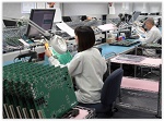
Depending on the technology, the challenge can be as simple as making minor design changes, which actually can happen at the Ger ber level versus requiring a significant revision to the board in question. First let’s conquer the simple. For analog, RF, and lower technology digital boards, the approach is the simplest. Typically, straightforward flying probe test is the answer. The better EMS companies use a dual-sided flying probe tester as shown in Figure 1. For this test approach, the test engineer simply asks that the vias not be covered with soldermask, which can be a simple change handled at the CAM/Gerber level. Because flying probe testers can generally test a via with a 20 mil pad and a 10 mil hole, the holes do not need to be plated shut. Depending on the test coverage, the test department may recommend adding vias, assuming the design can handle it from an electrical perspective.
Editor’s Note: This article originally appeared in the March 2016 issue of The PCB Magazine.
Share on:


Suggested Items
Koh Young Showcases Award-winning Inspection Solutions at SMTconnect with SmartRep in Hall 4A.225
04/25/2024 | Koh Young TechnologyKoh Young Technology, the industry leader in True 3D measurement-based inspection solutions, will showcase an array of award-winning inspection and measurement solutions at SMTconnect alongside its sales partner, SmartRep, in booth 4A.225 at NürnbergMesse from June 11-13, 2023. The following offers a glimpse into what Koh Young will present at the tradeshow:
Real Time with… IPC APEX EXPO 2024: Plasmatreat: Innovative Surface Preparation Solutions
04/25/2024 | Real Time with...IPC APEX EXPOIn this interview, Editor Nolan Johnson speaks with Hardev Grewal, CEO and president of Plasmatreat, a developer of atmospheric plasma solutions. Plasmatreat uses clean compressed air and electricity to create plasma, offering environmentally friendly methods for surface preparation. Their technology measures plasma density for process optimization and can remove organic micro-contamination. Nolan and Hardev also discuss REDOX-Tool, a new technology for removing metal oxides.
Nanotechnology Market to Surpass $53.51 Billion by 2031
04/25/2024 | PRNewswireSkyQuest projects that the nanotechnology market will attain a value of USD 53.51 billion by 2031, with a CAGR of 36.4% over the forecast period (2024-2031).
Cadence, TSMC Collaborate on Wide-Ranging Innovations to Transform System and Semiconductor Design
04/25/2024 | Cadence Design SystemsCadence Design Systems, Inc. and TSMC have extended their longstanding collaboration by announcing a broad range of innovative technology advancements to accelerate design, including developments ranging from 3D-IC and advanced process nodes to design IP and photonics.
SMC Korea 2024 to Highlight Semiconductor Materials Trends and Innovations on Industry’s Path to $1 Trillion
04/24/2024 | SEMIWith Korea a major consumer of semiconductor materials and advanced materials a key driver of innovation on the industry’s path to $1 trillion, industry leaders and experts will gather at SMC (Strategic Materials Conference) Korea 2024 on May 29 at the Suwon Convention Center in Gyeonggi-do, South Korea to provide insights into the latest materials developments and trends. Registration is open.