-

- News
- Books
Featured Books
- smt007 Magazine
Latest Issues
Current Issue
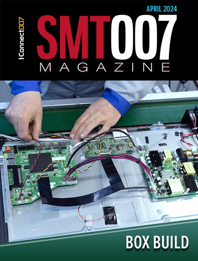
Box Build
One trend is to add box build and final assembly to your product offering. In this issue, we explore the opportunities and risks of adding system assembly to your service portfolio.

IPC APEX EXPO 2024 Pre-show
This month’s issue devotes its pages to a comprehensive preview of the IPC APEX EXPO 2024 event. Whether your role is technical or business, if you're new-to-the-industry or seasoned veteran, you'll find value throughout this program.

Boost Your Sales
Every part of your business can be evaluated as a process, including your sales funnel. Optimizing your selling process requires a coordinated effort between marketing and sales. In this issue, industry experts in marketing and sales offer their best advice on how to boost your sales efforts.
- Articles
- Columns
Search Console
- Links
- Events
||| MENU - smt007 Magazine
Solder Paste Exploration
June 2, 2016 | Stephen Las Marias, I-Connect007Estimated reading time: 1 minute
The trend towards miniaturization and increasing complexity of board assemblies as more functionality is being packed in smaller and smaller electronics devices no doubt continues to be among the critical issues in the electronics assembly industry today. Not to mention the ever-shrinking component sizes that are further complicating the manufacturing challenges.
To improve the electronics manufacturing process considering the challenges above, we have to drill down to the specific issues that have the greatest impact on the assembly line. And what better way to know these issues than to ask our readers?
So for this month's issue of SMT Magazine, we did a survey to find out the biggest factors affecting the electronics assembly process as the industry moves to tighter and tighter tolerances (finer lines and spaces). In our survey, we found out that while the most common line and space widths range from 2 mils to 5 mils, some respondents said they are doing boards with line and space widths down to 1 mil.
Given such tighter tolerances, respondents say PCBA testing and inspection, and soldering—in particular, solder paste printing—are their greatest challenge when it comes to electronics assembly.
This led me to what I would call my "solder paste printing exploration." From the manufacturers of solder pastes, to equipment makers, all the way to the solder paste inspection guys—and most importantly the electronics assemblers themselves who are using these products—I talked to the "supply chain," so to speak, all the way from Shanghai (during the recent NEPCON China 2016 exhibition in April) to our science and technology parks here in the Philippines, to find out what’s going on in the solder paste printing process, what factors impact the process, the challenges, and the best practices to consider to be able to address those challenges and improve efficiencies and yield in the SMT line.
Editor's Note: This article originally appeared in the June 2016 issue of SMT Magazine.
Suggested Items
Real Time with… IPC APEX EXPO 2024: Plasmatreat: Innovative Surface Preparation Solutions
04/25/2024 | Real Time with...IPC APEX EXPOIn this interview, Editor Nolan Johnson speaks with Hardev Grewal, CEO and president of Plasmatreat, a developer of atmospheric plasma solutions. Plasmatreat uses clean compressed air and electricity to create plasma, offering environmentally friendly methods for surface preparation. Their technology measures plasma density for process optimization and can remove organic micro-contamination. Nolan and Hardev also discuss REDOX-Tool, a new technology for removing metal oxides.
Real Time with... IPC APEX EXPO 2024: Advancements in Laser Depaneling with LPKF
04/24/2024 | Real Time with...IPC APEX EXPOJake Benz, LPKF sales manager for North America, discusses the company's advancements in laser depaneling. LPKF has introduced a green wavelength laser for processing rigid FR-4 circuit boards, bringing significant gains in processing speeds to market. The company transitioned from IR CO2 to UV wavelength due to heat and burning issues.
Hentec/RPS Publishes an Essential Guide to Selective Soldering Processing Tech Paper
04/17/2024 | Hentec Industries/RPS AutomationHentec Industries/RPS Automation, a leading manufacturer of selective soldering, lead tinning and solderability test equipment, announces that it has published a technical paper describing the critical process parameters that need to be optimized to ensure optimal results and guarantee the utmost in end-product quality.
IPC Design Competition: On Your Mark, Get Set, Go!
04/10/2024 | Andy Shaughnessy, Design007 MagazineI recently spoke with IPC’s Patrick Crawford, manager of design standards and related industry programs, and Kris Moyer, certified IPC master instructor, about this year’s IPC Design Competition. Now in its third year, the preliminary heat began in January, and the winners will compete in the final heat at IPC APEX EXPO in Anaheim.
DRAM Manufacturers Gradually Resume Production, Impact on Total Q2 DRAM Output Estimated to Be Less Than 1%
04/10/2024 | TrendForceFollowing in the wake of an earthquake that struck on April 3rd, TrendForce undertook an in-depth analysis of its effects on the DRAM industry, uncovering a sector that has shown remarkable resilience and faced minimal interruptions.


