-

- News
- Books
Featured Books
- smt007 Magazine
Latest Issues
Current Issue
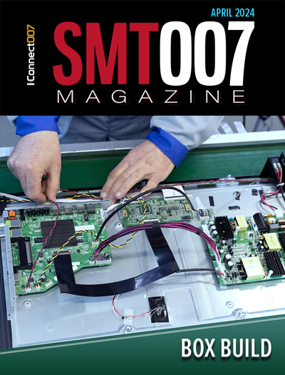
Box Build
One trend is to add box build and final assembly to your product offering. In this issue, we explore the opportunities and risks of adding system assembly to your service portfolio.

IPC APEX EXPO 2024 Pre-show
This month’s issue devotes its pages to a comprehensive preview of the IPC APEX EXPO 2024 event. Whether your role is technical or business, if you're new-to-the-industry or seasoned veteran, you'll find value throughout this program.

Boost Your Sales
Every part of your business can be evaluated as a process, including your sales funnel. Optimizing your selling process requires a coordinated effort between marketing and sales. In this issue, industry experts in marketing and sales offer their best advice on how to boost your sales efforts.
- Articles
- Columns
Search Console
- Links
- Events
||| MENU - smt007 Magazine
Solder Paste Printing: A User’s Perspective
June 22, 2016 | Stephen Las Marias, I-Connect007Estimated reading time: 3 minutes
I recently sat down with Integrated Micro-Electronics' Joemar Apolinario, engineering manager; Aurelio Bantigue, DFM engineer; and Rodney Bebe, process engineer, to get their insights on the solder paste printing process. They discussed the challenges and key considerations to make when dealing with tighter tolerances and finer pitches in line with the continuing miniaturization trend in the electronics manufacturing industry. They also talked about the impact of solder pastes in the printing process, and the criteria for their selection and qualification. Finally, they highlighted design and process strategies to get the best solder paste printing results.
Stephen Las Marias: Please discuss the solder paste printing process and the challenges you face.
Joemar Apolinario: The solder paste printing process is the most challenging process in the SMT operation because majority of the defects—around 60 to 80%—are coming from this process. These include non-wetting, insufficient volume, and short (solder bridging). Factors that greatly impact the solder paste printing quality may vary from the stencil design, the solder paste type, the machine capability (parameters), setup and tooling, and even the engineering skills of those who handle this process.
The challenge is that the devices now are getting smaller and smaller. We also have the complex products—those boards that combine critical components such as BGAs and ICs, which require finer pitches and smallest diameters—and non-critical components. The third challenge is the reliability. We have products that require higher reliability—and those are very sensitive to solder cracks or voiding defects. For most of the defects that we have encountered, the solder volume being deposited to the pad does not meet the requirement.
Joemar Apolinario, Aurelio Bantigue, and Rodney Bebe, IMI
Las Marias: How do you address those challenges?
Aurelio Bantigue: From a DFM standpoint, what we have done so far is we review the stencil design or the aperture design for each of the components. In our view, we consider both the PCB design and the components that will be mounted to the board. We recognize that the trend is toward smaller components, and the challenge is the appropriate aperture design for smaller pins and pads. What we can do is consider the appropriate solder volume. But the more challenging issue is the complexity—you are mixing small components, and larger components that require more solder paste, in a board. So, it will be more difficult. There are several design considerations that we do. We can do electroform step stencils, or sometimes, we have to overprint the solder paste—you have the solder paste outside the pad, you will have enough volume for those larger components. We can deposit small volume for the small components and enough volume for the larger components.
Las Marias: How does the solder paste impact the printing process?
Apolinario: The solder paste has a big impact on printing as it is the main ingredient of the process and it has a direct impact on reliability. The choice of the right type and composition of solder paste may help achieve good printing quality. But, the key here is having the right parameter to use, for instance, the design of the pad and the stencil. We need to select the appropriate type of solder to match the stencil design and pad design to have a good printing result. Another factor is the machine. We need to use the appropriate machine to get good results.
We have different types of solder printing machines—we have the screen printing as our typical printing method; we are now also using jet printing process. So, that’s the factor. Apart from the multi-step stencil design to accommodate those complex PCBAs, we are now trying electroform nano-coated stencil. This is something new in our process—nano-coating by immersion coating process. The design of the stencil is electroformed, then it goes through a nano-coating process. This process makes the stencil smoother and non-sticky, to have a good transfer efficiency and to reduce cleaning sequence in the process.
Editor's Note: This article originally appeared in the June 2016 issue of SMT Magazine.
Suggested Items
Real Time with… IPC APEX EXPO 2024: Plasmatreat: Innovative Surface Preparation Solutions
04/25/2024 | Real Time with...IPC APEX EXPOIn this interview, Editor Nolan Johnson speaks with Hardev Grewal, CEO and president of Plasmatreat, a developer of atmospheric plasma solutions. Plasmatreat uses clean compressed air and electricity to create plasma, offering environmentally friendly methods for surface preparation. Their technology measures plasma density for process optimization and can remove organic micro-contamination. Nolan and Hardev also discuss REDOX-Tool, a new technology for removing metal oxides.
Real Time with... IPC APEX EXPO 2024: Advancements in Laser Depaneling with LPKF
04/24/2024 | Real Time with...IPC APEX EXPOJake Benz, LPKF sales manager for North America, discusses the company's advancements in laser depaneling. LPKF has introduced a green wavelength laser for processing rigid FR-4 circuit boards, bringing significant gains in processing speeds to market. The company transitioned from IR CO2 to UV wavelength due to heat and burning issues.
Hentec/RPS Publishes an Essential Guide to Selective Soldering Processing Tech Paper
04/17/2024 | Hentec Industries/RPS AutomationHentec Industries/RPS Automation, a leading manufacturer of selective soldering, lead tinning and solderability test equipment, announces that it has published a technical paper describing the critical process parameters that need to be optimized to ensure optimal results and guarantee the utmost in end-product quality.
IPC Design Competition: On Your Mark, Get Set, Go!
04/10/2024 | Andy Shaughnessy, Design007 MagazineI recently spoke with IPC’s Patrick Crawford, manager of design standards and related industry programs, and Kris Moyer, certified IPC master instructor, about this year’s IPC Design Competition. Now in its third year, the preliminary heat began in January, and the winners will compete in the final heat at IPC APEX EXPO in Anaheim.
DRAM Manufacturers Gradually Resume Production, Impact on Total Q2 DRAM Output Estimated to Be Less Than 1%
04/10/2024 | TrendForceFollowing in the wake of an earthquake that struck on April 3rd, TrendForce undertook an in-depth analysis of its effects on the DRAM industry, uncovering a sector that has shown remarkable resilience and faced minimal interruptions.


