


 Standard of Excellence: Collaboration—The Right Path to Innovation
 Global Sourcing Spotlight: Golf, Friedman, and the Benefits of Global Sourcing
 Nolan’s Notes: Coming to Terms With AI
2D X-ray Inspection With Materials and Thickness Identification
June 7, 2017 | Paul D. Scott, Ph.D., IBEX Innovations, and Evstatin Krastev, Ph.D., P.E., Nordson DageEstimated reading time: 7 minutes
ABSTRACT
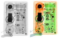
X-ray inspection systems are key tools for quality control, yield enhancement, and failure analysis of PCBs and semiconductor devices. In many cases, these capable tools provide the only non-destructive techniques for inspection of electronic components. There have been significant improvements in the X-ray inspection capabilities (both 2D and 3D) in the last several years. In this paper we report a new development that permits material and thickness information to be obtained via 2D X-ray inspection.
While absorption contrast X-ray imaging is a very powerful inspection technique, it does not exploit all of the information present within the X-ray beam transmitted through a sample. A new technology has been recently developed that, instead of simply measuring the total absorption of the X-ray beam, also enables changes in the beam energy to be resolved. This allows the effects of thickness and density to be decoupled, enabling both to be determined. This quantitative composition and thickness information can then be used to provide new levels of insight in PCB and semiconductor inspection, potentially leading the way to a new generation of X-ray inspection technology.
It is quite straightforward to accommodate this technology in an existing 2D X-ray (2DX) inspection system. Advanced software algorithms need to be incorporated and an intuitive user interface is provided.
We present an overview of this new technology and give examples of other industries where this technology is being adopted, as well as example applications for the PCB and semiconductor industries.
INTRODUCTION
The need to inspect electronic components and assemblies non-destructively is the main driver behind the development and advancement of the X-ray inspection technology for the electronics industry. In many cases, X-Ray inspection (2D and 3D) provides the only non-destructive techniques to inspect optically hidden components and solder joints such as BGA, POP, QFN, flip chips, through holes, TSVs, microbumps, copper pillars, etc.
All X-ray inspection systems (2D and 3D) rely on absorption contrast imaging, where the contrast is generated by the stopping power of the sample. As such, higher density and/or thicker regions of a sample produce darker regions in a grey-scale image. X-ray inspection systems use this method to image features such as wire bonds and ball grid arrays down to a feature recognition size of 100 nm (0.1 μm).
While contrast imaging is a very powerful and widely used technique, there is significantly more information present within the X-ray beam, which, until now, has not been exploited in electronics inspection. Instead of simply measuring the total absorption of the X-ray beam, a physical structure known as a multi absorption plate (MAP) can be placed in the beam path. This, coupled with machine learning algorithms, enables material type and thickness information to be acquired alongside the standard grey-scale image.
Quantitative composition and thickness information can then be used to provide more detailed diagnostics in PCB and semiconductor inspection. Applications include, but are not limited to, analysis of solder types, track thickness measurements, and conformance to quality standards.
An overview of the theory behind the operation of the MAP is given below, as well as some simple examples showing the benefits of using the MAP technology to add additional capabilities to 2D X-Ray inspection. MAP technology also has applications in the security, medical and food processing industries. Nordson Dage has partnered with IBEX to bring the benefits of this technology to the electronics inspection, including inspection of PCBs and semiconductor devices. A range of examples is presented and the authors aim to start active discussions that would generate new needs and ideas for use of the technology for non-destructive inspection of electronics systems and components.
BASIC PRINCIPLES OF THE MAP TECHNOLOGY
X-ray Interaction with a Sample
X-rays are generated using a tungsten target which produces a continuous spectrum, known as Bremβtrahlung radiation, as well as characteristic peaks at specific energies.
Adding a sample such as a printed circuit board into the beam attenuates the X-ray spectrum in the following way:
I(E) = I0(E)exp(-µ(E)t) (1)
where I0(E) and I(E) are the intensities of the X-ray spectra before and after the sample, respectively; µ(E) is the material-dependent linear attenuation coefficient; and t is the thickness of the sample.
If I0(E) and I(E) can be determined, it is possible to extract the parameter µ(E) which relates to the material type and the material thickness.
A standard CMOS detector integrates the total energy deposited into each pixel over the user-selected integration time. As such, the detector is able to measure total energy deposited per pixel but not the actual energy spectrum. This means that it is not possible to decouple the material and thickness terms in equation (1), meaning that thin, high density materials are indistinguishable from thick, low density materials in a single 2D projection.
The Multi Absorption Plate (MAP) acts like a complex color filter for the X-rays by imposing a repeating modulation to the X-ray beam over a few neighboring pixels. This modulation results in a variation in the energy distribution of the X-ray beam incident on the neighboring pixels in a way that enables unique materials information to be obtained.
Extracting Materials Information—Simple Examples
Figure 1 shows the word IBEX constructed using a series of copper tiles with a background made up of foils of silver. The thicknesses of the foils have been selected in order to randomize the grey-scale intensity transmitted by the tiles and hence obscure the word IBEX in a standard X-ray image. Analyzing the image with a MAP in place recovers the materials information. The intensities of the coloring in the bottom image of Figure 1 reflect the relative thicknesses of the tiles.
Figure 1: Optical image showing the word IBEX created as a mosaic of random thicknesses of silver and copper foils (top); X-ray transmission image showing that it is not possible to distinguish between the foils using absorption contrast alone (middle); materials contrast image showing that the missing information can be recovered using the MAP (bottom).
This materials information can be displayed to the user in terms of a basic mask identifying the materials, as an overlay of material identification on the absorption contrast image, or in the case of automated quality inspection systems as a pass/fail criterion.
Page 1 of 2
Share on:


Suggested Items
Indium Experts to Present on High-Temperature, Lead-Free Solder Paste and High Reliability Liquid Metal Alloys Poster at ECTC
05/16/2024 | Indium CorporationIndium Corporation Research Associate Kyle Aserian will deliver a presentation at the 74th Electronic Components and Technology Conference (ECTC) on May 31, in Denver, Colorado.
Indium Experts to Present at Electronics in Harsh Environments SMTA Conference
05/13/2024 | Indium Corporationndium Corporation Technical Manager for Europe, Africa, and the Middle East, Karthik Vijay, will deliver a technical presentation and Indium Corporation Senior Technologist, Dr. Ronald Lasky, will deliver both a workshop and technical presentation at the Electronics in Harsh Environments SMTA Conference on May 14-16 in Copenhagen, Denmark.
Connect the Dots: Designing for Reality—The Pre-Manufacturing Process
05/08/2024 | Matt Stevenson -- Column: Connect the DotsI have been working with Nolan Johnson on a podcast series about designing PCBs for the reality of manufacturing. By sharing lessons learned over a long career in the PCB industry, we hope to shorten learning curves and help designers produce better boards with less hassle and rework. Episode 2 deals with the electronic pre-manufacturing process. Moving from CAD (computer-aided design) to CAM (computer-aided manufacturing) is a key step in PCB manufacturing. CAM turns digital designs into instructions that machines can use to actually build the PCB.
AIM Solder Signs Shinil Fl Ltd. as New Distributor for Korea
05/08/2024 | AIM SolderAIM Solder, a leading global manufacturer of solder assembly materials for the electronics industry, is pleased to announce a new distribution partnership with Shinil Fl Ltd., a prominent supplier of technological solutions in the SMT and semiconductor sectors.
Indium Corporation to Showcase HIA Materials at ECTC
05/07/2024 | Indium CorporationAs an industry leader in innovative materials solutions for semiconductor packaging and assembly, Indium Corporation® will feature its advanced products designed to meet the evolving challenges of heterogeneous integration and assembly (HIA) and fine-pitch system-in-package (SiP) applications at the 74th Electronic Components and Technology Conference (ECTC), May 28‒31, in Denver, Colorado.